 Current to voltage converter circuit can be made using a single resistor, it is very simple since any current will naturally develop a voltage when flow through a resistor. Using an active component, a small developed voltage on a resistor can be accurately measured since we can amplify it to reach a convenient level to …[Read More]
LF356 based Wide Range Current-To-Voltage Converter circuit
Current to voltage converter circuit can be made using a single resistor, it is very simple since any current will naturally develop a voltage when flow through a resistor. Using an active component, a small developed voltage on a resistor can be accurately measured since we can amplify it to reach a convenient level to …[Read More]Building the Automatic Etch-A-Sketch Controller

Overview
The classic toy Etch-A-Sketch has been written with a controller to see it move by itself.
Explanation
The pictures can be drawn automatically by showing up different angled lines caused by an order by the chip to the motors. The chip will have to connect to a computer using the UART in order to obtain several pictures. The knobs are connected to 2 stepper motors being controlled by an Atmel microcontroller.
The computer, microcontroller, stepper control, and Etch-A-Sketch are the 4 main sections in the setup. They have a small communication script in between each section as all 4 sections are relatively decoupled from each other. This design is in reference with the 7 layers of a standard computer network which are separated from each other.
The microcontroller program contains 3 functions where each is selected by one of the 3 buttons. The first button is a testing procedure that loads specified values in memory. The second button loads these values from the UART input. The third button handles sending the necessary voltages to the next step. The knobs on the Etch-A-Sketch are driven by using a couple of stepper motors.
Line-Following Autonomous Vehicle electronic project overview

Overview
The car is made to follow a non-predetermined path by following a line against a luminance contrasting surface that is detected by an array of sensors.
Explanation
An Atmel AVR8515 microcontroller is used by the car in order to have a complete control of the car by controlling the drive and steering servos. The microcontroller steers the car accordingly as it senses the position of the line in reference to the car. The wheel rotation is detected by a 6th light sensor which maintains constant speed. The data from the wheel is obtained by a digital feedback algorithm as the desired speed is maintained by adjusting the PWM signal to the motor.
The light reflectance is detected by the sensors and the floor is illuminated by each of 5-arrayed infrared LED. An output of 0V or 5V is the result of converting the output of the detectors. A higher reflectance surface indicates white line due to low output while a black line below a sensor is indicated by a high output.
A LED-sensor pair is mounted facing the wheel which detects the speed of the car. It also detects the position of wheel.
LED Pilot Light (LEDs (Light Emitting Diode) part are interesting things. They only operate at VDC within specific tolerances,
LEDs (Light Emitting Diode) part are interesting things. They only operate at VDC within specific tolerances, and generally connected with a current limiting resistor towards the power source. Rather than a resistor, it is possible to use a FET (Field Effect Transistor) like the ECG31 and, NTE312 (you may try other types).

When the gate and the source are connected together, it acts as a current regulator.
In the circuit above, the current is constant between 6 and 8 mA at 5 to 30Vdc.If the diode is added (the 1N4148 is optional), this circuit is secured agains polarity reversal and can be connected to a AC power supply of 5 to 20 VAC.
Circuit designed by Tony Van Roon
LM741 bassed Active High Pass Filter circuit with exxplanation
This is active high pass filter circuit for 327Hz frequency using LM741. It will use to build Harmonic at 3 of 130.81 frequency have the value at least. More than the frequency Fundamental 30 dB, for output be sawtooth wave form for use in sound of music way system Electronic design will use the circuit filters three rank frequency. By have 3 dB you slopes can use Op-amp IC number LM741 or number LF351it will meet the frequency well.
Circuit diagram:
Circuit diagram:

Active High Pass Filter Circuit Diagram
Source: ElecCircuitVoice Bandwidth Filter circuit and explanation
This circuit passes frequencies in the 300Hz - 3.1kHz range, as present in human speech. The circuit consists of cascaded high-pass and low-pass filters, which together form a complete band-pass filter. One half of a TL072 dual op amp (IC1a) together with two capacitors and two resistors make up a second-order Sallen-Key high-pass filter. With the values shown, the cut-off frequency (3dB point) is around 300Hz. As the op amp is powered from a single supply rail, two 10kO resistors and a 10µF decoupling capacitor are used to bias the input (pin 5) to one-half supply rail voltage.
Circuit diagram:
The output of IC1a is fed into the second half of the op amp (IC1b), also configured as a Sallen-Key filter. However, this time a low-pass function is performed, with a cut-off frequency of about 3.1kHz. The filter component values were chosen for Butterworth response characteristics, providing maximum pass-band flatness. Overall voltage gain in the pass-band is unity (0dB), with maximum input signal level before clipping being approximately 3.5V RMS. The 560O resistor at IC1b's output provides short-circuit protection.
Circuit diagram:

Voice Bandwidth Filter Circuit Diagram
The output of IC1a is fed into the second half of the op amp (IC1b), also configured as a Sallen-Key filter. However, this time a low-pass function is performed, with a cut-off frequency of about 3.1kHz. The filter component values were chosen for Butterworth response characteristics, providing maximum pass-band flatness. Overall voltage gain in the pass-band is unity (0dB), with maximum input signal level before clipping being approximately 3.5V RMS. The 560O resistor at IC1b's output provides short-circuit protection.
Author: M. Sharp - Copyright: Silicon Chip Electronics
Simple Function Generator circuit
Simple triangle-wave generators have a weakness in that the waveform of their output signal normally cannot be modified. The circuit presented here makes it possible to smoothly alter the waveform of a linearly rising and steeply trailing saw-tooth signal through a symmetrical triangle-wave to a slowly trailing, steeply rising linear sawtooth. The wanted waveform may be selected independently of the frequency, which can also be varied uniformly from 0.2 Hz to 8 kHz. At the same time, a rectangular signal with variable duty cycle (also independent of frequency) is available at the rectangular-signal output of the circuit.
The circuit consists of integrator IC1b, whose output is applied to comparator IC1c. The output of the comparator is a rectangular signal The output of IC1b is raised by amplifier IC1d to a level that allows the full output voltage range of the operational amplifier to be used. Op amp IC1a provides a stable virtual earth, whose level is set to half the supply voltage with P1. The smooth setting of the frequency is made possible by feedback of part of the output of the comparator to the input of the integrator via P2. This preset is usually not provided in standard triangle-wave generators. Network D1-R1-D2-R2-P3 makes it possible to give integrator capacitor C3 different charging and discharge times.

This arrangement enables the output signal at A1 and the duty cycle of the rectangular wave signal at A2 to be varied. Varying the amplification factor with P5 has no effect on the frequency set with P2. The slope of the signal edges, the transient responses, and the output voltage range (rail-to-rail or with some voltage drop) depend on the type of op amp used. The TL084 used in the prototype offers a good compromise between price and meeting the wanted parameters. The circuit is best built on a small piece of prototyping board. The circuit draws a current of not more than 12 mA.
Brief parameters:
Provides triangle-wave, sawtooth or rectangular signal
Waveform variable independently of frequency (triangle wave and sawtooth)
Duty cycle of rectangular signal can be set independently of frequency
Applications:
Test and measurement
Pulse-width control
Summary of preset action:
P1 – sets virtual earth to a level equal to Ucc/2;
P2 – sets the frequency;
P3– sets the waveform;
P4 – sets the hysteresis of the comparator (frequency and amplitude of the triangle-wave signal)
P5 – sets the amplification of the triangle-wave and sawtooth signals.
The circuit consists of integrator IC1b, whose output is applied to comparator IC1c. The output of the comparator is a rectangular signal The output of IC1b is raised by amplifier IC1d to a level that allows the full output voltage range of the operational amplifier to be used. Op amp IC1a provides a stable virtual earth, whose level is set to half the supply voltage with P1. The smooth setting of the frequency is made possible by feedback of part of the output of the comparator to the input of the integrator via P2. This preset is usually not provided in standard triangle-wave generators. Network D1-R1-D2-R2-P3 makes it possible to give integrator capacitor C3 different charging and discharge times.

Simple Function Generator Circuit Diagram
This arrangement enables the output signal at A1 and the duty cycle of the rectangular wave signal at A2 to be varied. Varying the amplification factor with P5 has no effect on the frequency set with P2. The slope of the signal edges, the transient responses, and the output voltage range (rail-to-rail or with some voltage drop) depend on the type of op amp used. The TL084 used in the prototype offers a good compromise between price and meeting the wanted parameters. The circuit is best built on a small piece of prototyping board. The circuit draws a current of not more than 12 mA.
Brief parameters:
Provides triangle-wave, sawtooth or rectangular signal
Waveform variable independently of frequency (triangle wave and sawtooth)
Duty cycle of rectangular signal can be set independently of frequency
Applications:
Test and measurement
Pulse-width control
Summary of preset action:
P1 – sets virtual earth to a level equal to Ucc/2;
P2 – sets the frequency;
P3– sets the waveform;
P4 – sets the hysteresis of the comparator (frequency and amplitude of the triangle-wave signal)
P5 – sets the amplification of the triangle-wave and sawtooth signals.
Very Low Power 32kHz Oscillator
The 32-kHz low-power clock oscillator offers numerous advantages over conventional oscillator circuits based on a CMOS inverter. Such inverter circuits present problems, for example, supply currents fluctuate widely over a 3V to 6V supply range, while current consumption below 250 µA is difficult to attain. Also, operation can be unreliable with wide variations in the supply voltage and the inverter’s input characteristics are subject to wide tolerances and differences among manufacturers. The circuit shown here solves the above problems. Drawing just 13 µA from a 3V supply, it consists of a one-transistor amplifier/oscillator (T1) and a low-power comparator/reference device (IC1).
Circuit diagram:
The base of T1 is biased at 1.25 V using R5/R4 and the reference in IC1. T1 may be any small-signal transistor with a decent beta of 100 or so at 5 µA (defined here by R3, fixing the collector voltage at about 1 V below Vcc). The amplifier’s nominal gain is approximately 2 V/V. The quartz crystal combined with load capacitors C1 and C3 forms a feedback path around T1, whose 180 degrees of phase shift causes the oscillation. The bias voltage of 1.25 V for the comparator inside the MAX931 is defined by the reference via R2. The comparator’s input swing is thus accurately centred around the reference voltage.
Operating at 3 V and 32 kHz, IC1 draws just 7 µA. The comparator output can source and sink 40 mA and 5 mA respectively, which is ample for most low-power loads. However, the moderate rise/fall times of 500 ns and 100 ns respectively can cause standard, high-speed CMOS logic to draw higher than usual switching currents. The optional 74HC14 Schmitt trigger shown at the circuit output can handle the comparator’s rise/fall times with only a small penalty in supply current.
Author: D. Prabakaran - Copyright: 2004 Elekto
Circuit diagram:

Very Low Power 32kHz Oscillator Circuit Diagram
The base of T1 is biased at 1.25 V using R5/R4 and the reference in IC1. T1 may be any small-signal transistor with a decent beta of 100 or so at 5 µA (defined here by R3, fixing the collector voltage at about 1 V below Vcc). The amplifier’s nominal gain is approximately 2 V/V. The quartz crystal combined with load capacitors C1 and C3 forms a feedback path around T1, whose 180 degrees of phase shift causes the oscillation. The bias voltage of 1.25 V for the comparator inside the MAX931 is defined by the reference via R2. The comparator’s input swing is thus accurately centred around the reference voltage.
Operating at 3 V and 32 kHz, IC1 draws just 7 µA. The comparator output can source and sink 40 mA and 5 mA respectively, which is ample for most low-power loads. However, the moderate rise/fall times of 500 ns and 100 ns respectively can cause standard, high-speed CMOS logic to draw higher than usual switching currents. The optional 74HC14 Schmitt trigger shown at the circuit output can handle the comparator’s rise/fall times with only a small penalty in supply current.
Author: D. Prabakaran - Copyright: 2004 Elekto
TIP 2955 bassed REGULATOR 12 VOLT 15 AMPRE
This is circuit of adapter/ regulator 12V that can deliver up to 15 A of current. The common voltage regulator IC 7812(IC1) is used to keep the voltage at steady 12V and three TIP 2599 power transistors in parallel are wired in series pass mode to boost the output current. The 7812 can provide only up to 1A and rest of the current is supplied by the series pass transistors. The 15A bridge B1 does the job of rectifying the stepped down AC input. The capacitor C1, C2 and C3 act as filters. The 1A fuse F1 protects the IC1 from over current in case if the pass transistors fail. The 15A fuse F2 protects the entire circuit (especially the pass transistors) from over current.
With high current transformer, power transistors and high current bridge the circuit is a bit costly and you may try this only if there is a serious need.
 Skema Rangkaia Regulator 12 volt 15 A
Note:
Features IC 78xx
Output current in excess of 1A
Internal thermal overload protection
No external components required
Output transistor safe area protection
Internal short circuit current limit
Available in the aluminum TO-3 package

Gambar IC regulator 7812
Voltage Range IC 78xx
LM7805C 5V
LM7812C 12V
LM7815C 15V
The LM78XX series of three terminal regulators is available with several fixed output voltages making them useful in a wide range of applications. One of these is local on card regulation, eliminating the distribution problems associated with single point regulation. The voltages available allow these regulators to be used in logic systems, instrumentation, HiFi, and other solid state electronic equipment. Although designed primarily as fixed voltage regulators these devices can be used with external components to obtain adjustable voltages and currents.
Considerable effort was expanded to make the LM78XX series of regulators easy to use and minimize the number of external components. It is not necessary to bypass the output, although this does improve transient response. Input bypassing is needed only if the regulator is located far from the filter capacitor of the power supply.
With high current transformer, power transistors and high current bridge the circuit is a bit costly and you may try this only if there is a serious need.
 Skema Rangkaia Regulator 12 volt 15 A
Note:
The T1 can be a 230V AC primary, 18V secondary, 15A type transformer.
The B1 can be a 15A bridge.
If 15A Bridge is not available, make one using four RURG1520CC diodes.
The IC1 and transistors must be mounted on heat sinks.
The B1 can be a 15A bridge.
If 15A Bridge is not available, make one using four RURG1520CC diodes.
The IC1 and transistors must be mounted on heat sinks.
Features IC 78xx
Output current in excess of 1A
Internal thermal overload protection
No external components required
Output transistor safe area protection
Internal short circuit current limit
Available in the aluminum TO-3 package

Gambar IC regulator 7812
Voltage Range IC 78xx
LM7805C 5V
LM7812C 12V
LM7815C 15V
The LM78XX series of three terminal regulators is available with several fixed output voltages making them useful in a wide range of applications. One of these is local on card regulation, eliminating the distribution problems associated with single point regulation. The voltages available allow these regulators to be used in logic systems, instrumentation, HiFi, and other solid state electronic equipment. Although designed primarily as fixed voltage regulators these devices can be used with external components to obtain adjustable voltages and currents.
Considerable effort was expanded to make the LM78XX series of regulators easy to use and minimize the number of external components. It is not necessary to bypass the output, although this does improve transient response. Input bypassing is needed only if the regulator is located far from the filter capacitor of the power supply.
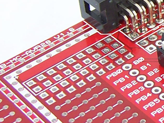
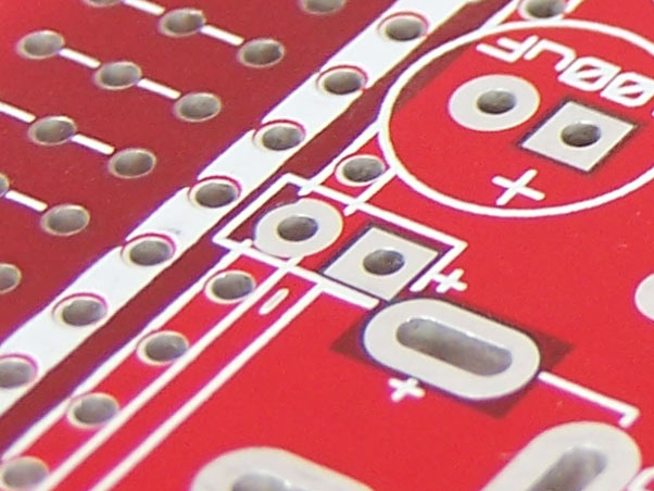
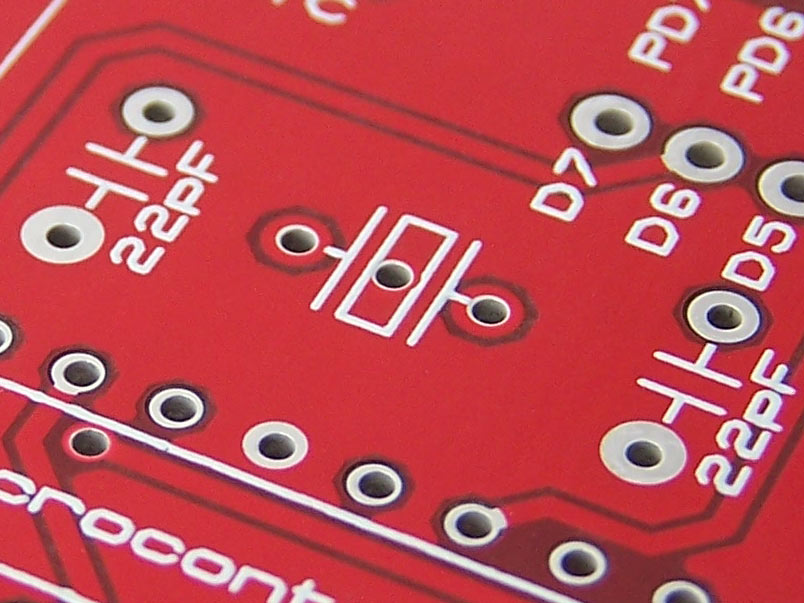
28 Pin AVR Development Board Version 1.6 is now released
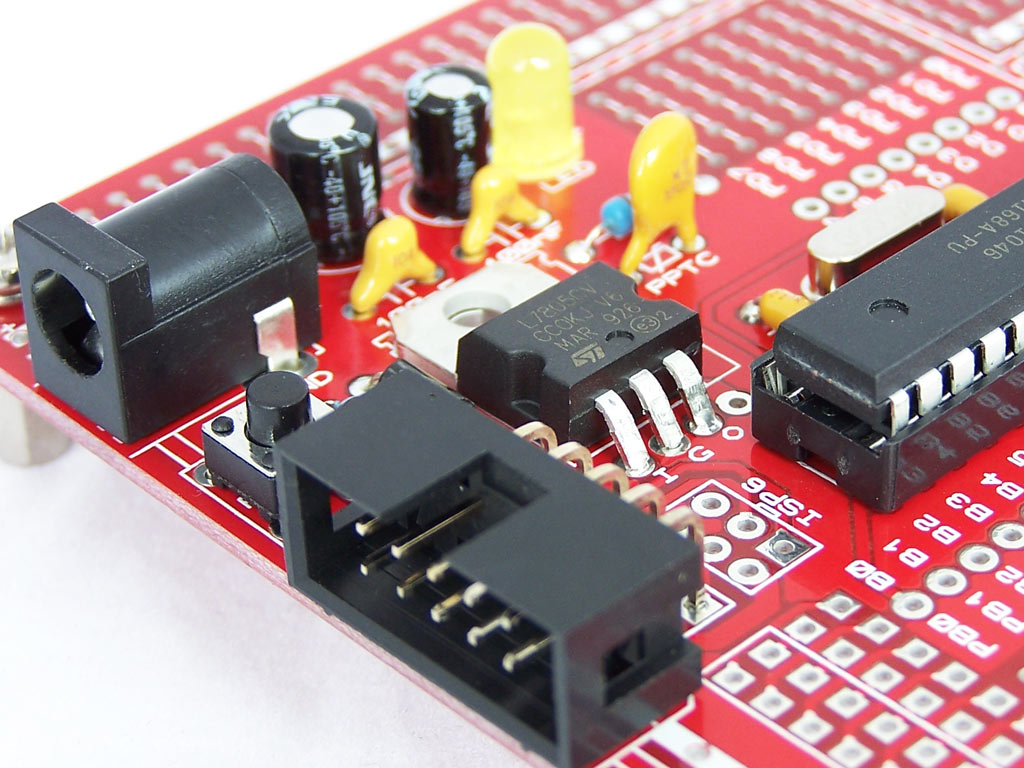
protostack.com released the 28 Pin AVR Development Board back in 2008 and since then it has gone through many iterations. This week they release version 1.6 which adds 4 improvements.
What has changed?
1- The size of the IDC/Dual row area has been increased from 2×8 to 2×9 holes. 
2- They added square and circular pads on the top layer for polarised headers. The main reason for this was to make them stand out more. Functionally they are unchanged.

some labels for the ISP-10 connector are added

Crystal oscillator holes now have pads only only on the bottom layer. This fixes a problem where the oscillator case was making contact with the pads.

The board is available by itself for $9.60, as part of an ATMEGA8A Development Kit ($18.50) or as part of an ATMEGA168A Development Kit ($19.80)
2- They added square and circular pads on the top layer for polarised headers. The main reason for this was to make them stand out more. Functionally they are unchanged.
some labels for the ISP-10 connector are added

Crystal oscillator holes now have pads only only on the bottom layer. This fixes a problem where the oscillator case was making contact with the pads.
The board is available by itself for $9.60, as part of an ATMEGA8A Development Kit ($18.50) or as part of an ATMEGA168A Development Kit ($19.80)
L4970A bassed Data Sheet Ic Switching circuit and explanation
IC L4970A DESCRIPTION
variable from 5.1 to 40V. Realized with BCD mixed technology, the device uses a DMOS output transistor to obtain very high efficiency and very fast switching times. Features of the L4970A include reset and power fail for microprocessors, feed forward line regulation, soft start, limiting current and thermal protection. The device is mounted in a 15-lead multiwatt plastic power package and requires few external components. Efficient operation at switching frequencies up to 500KHz allows reduction in the size and cost of external filter components. This is advanced information on a new product now in development or undergoing evaluation. Details are subject to change without notice.
June 2000

FEATURE IC L4970A
- 10A OUTPUT CURRENT
- 5.1V TO 40V OUTPUT VOLTAGERANGE
- 0 TO 90% DUTY CYCLE RANGE
- INTERNAL FEED-FORWARD LINE REGULATION
- INTERNAL CURRENT LIMITING
- PRECISE 5.1V ± 2% ON CHIP REFERENCE
- RESET AND POWER FAIL FUNCTIONS
- SOFT START
- INPUT/OUTPUT SYNC PIN
- UNDER VOLTAGE LOCK OUT WITH HYSTERETIC
- TURN-ON
- PWM LATCH FOR SINGLE PULSE PER PERIOD
- VERYHIGH EFFICIENCY
- SWITCHING FREQUENCY UP TO 500KHz
- THERMAL SHUTDOWN
- CONTINUOUS MODE OPERATION
ABSOLUTE MAXIMUM RATINGS IC L4970A

IC L4970A PIN FUNCTIONS


5.1V / 10A Low Cost Application IC L4970A

10A Switching Regulator, Adjustable from 0V to 25V IC L4970A

LM2678-5.0 bassed 5 Volt Switching Regulator Circuit and explanation
This is the circuit diagram of a 5V switching regulator based on the IC LM2678. The LM2678 series of regulators are monolithic integrated circuits which provide all necessary functions required for a buck switching regulator and can drive up to 5A loads. The IC has more than 90% efficiency and has excellent load and line regulation. The LM2678 is available in three fixed output voltages (3.3V, 5V, 12V) and an adjustable output version. The IC is also packed with a handful l of features like thermal shutdown, current limiting and ON/OFF control.
 Skema Rangkaian 5 Volt Switching Regulator LM2678-5.0
 LM2678-5.0 Pinout
Note:
- The circuit given here is based on the version LM2678-5.0 which gives an output of 5V.
- The power supply for the circuit can be anything between 8 to 40V DC.
- The feedback wiring must be placed as away as possible from the inductor L1.
- Do not use loads that consume more than 5A.
- A heat sink is seriously recommended for the IC.
power supplay +12 dan - 12 Dual Regulator
This is of a dual regulated that provides +12V and -12V from the AC mains. A regulator like this is a very essential tool on the work bench of an electronic hobbyist.
Transformer T1 steps down the AC mains voltage and diodes D1, D2, D3 and D4 does the job of rectification. Capacitors C1 and C2 does of filtering.C3, C4, C7and C8 are decoupling capacitors. IC 7812 and 7912 are used for the purpose of voltage regulation in which the former is a positive 12V regulator and later is a negative 12V regulator. The output of 7812 will be +12V and that of 7912 will be -12V.
 Skema Rangkaian Dual Regulator power supplay
Use Transformer 15-0-15 V, 1A secondary step-down transformer.
Capacitor C1,C2,C5 and C6 must be rated 50V or more.
IC regulator 78xx (7812) Description
The LM78XX series of three terminal regulators is available with several fixed output voltages making them useful in a wide range of applications. One of these is local on card regulation, eliminating the distribution problems associated with single point regulation.

Features IC LM7812
Output current in excess of 1A
Output Voltages of 5, 6, 8, 9, 10, 12, 15, 18 , 24V
Internal thermal overload protection
No external components required
Output transistor safe area protection
Internal short circuit current limit
Absolute Maximum Ratings IC LM7812
Input Voltage (VO = 5V, 12V and 15V) : 35V
Operating Temperature Range (TA) : 0°C to +70°C
Maximum Junction Temperature : 150°C
Storage Temperature Range −65°C to +150°C
Lead Temperature (Soldering, 10 sec.)
IC regulator 79xx (7912) Description
The LM79XX series of three-terminal negative regulators are available with several fixed output voltages, making them useful in a wide range of applications. Each type employs internal current limiting, thermal shutdown and safe operating area protection, making it essentially indestructible.

Features IC LM7912
• Output Current in Excess of 1A
• Output Voltages of -5, -6, -8, -9, -10, -12, -15, -18 , -24V
• Internal Thermal Overload Protection
No external components required
• Short Circuit Protection
• Output Transistor Safe Operating Area Compensation
Absolute Maximum Ratings IC LM7912
Input Voltage (VO = -5V, to 15V) : 35V
Operating Temperature Range (TA) : 0°C to +70°C
Maximum Junction Temperature : 150°C
Storage Temperature Range −65°C to +150°C
Lead Temperature (Soldering, 10 sec.).
TIP 2955 bassed REGULATOR 12 VOLT 15 AMPRE circuit and explanation
This is circuit of adapter/ regulator 12V that can deliver up to 15 A of current. The common voltage regulator IC 7812(IC1) is used to keep the voltage at steady 12V and three TIP 2599 power transistors in parallel are wired in series pass mode to boost the output current. The 7812 can provide only up to 1A and rest of the current is supplied by the series pass transistors. The 15A bridge B1 does the job of rectifying the stepped down AC input. The capacitor C1, C2 and C3 act as filters. The 1A fuse F1 protects the IC1 from over current in case if the pass transistors fail. The 15A fuse F2 protects the entire circuit (especially the pass transistors) from over current.
With high current transformer, power transistors and high current bridge the circuit is a bit costly and you may try this only if there is a serious need.
Skema Rangkaia Regulator 12 volt 15 ANote:
The T1 can be a 230V AC primary, 18V secondary, 15A type transformer.
The B1 can be a 15A bridge.
If 15A Bridge is not available, make one using four RURG1520CC diodes.
The IC1 and transistors must be mounted on heat sinks.
The B1 can be a 15A bridge.
If 15A Bridge is not available, make one using four RURG1520CC diodes.
The IC1 and transistors must be mounted on heat sinks.
Features IC 78xx
Output current in excess of 1A
Internal thermal overload protection
No external components required
Output transistor safe area protection
Internal short circuit current limit
Available in the aluminum TO-3 package
Gambar IC regulator 7812
Voltage Range IC 78xx
LM7805C 5V
LM7812C 12V
LM7815C 15V
The LM78XX series of three terminal regulators is available with several fixed output voltages making them useful in a wide range of applications. One of these is local on card regulation, eliminating the distribution problems associated with single point regulation. The voltages available allow these regulators to be used in logic systems, instrumentation, HiFi, and other solid state electronic equipment. Although designed primarily as fixed voltage regulators these devices can be used with external components to obtain adjustable voltages and currents.
Considerable effort was expanded to make the LM78XX series of regulators easy to use and minimize the number of external components. It is not necessary to bypass the output, although this does improve transient response. Input bypassing is needed only if the regulator is located far from the filter capacitor of the power supply.
Dynamic Microphone Preamplifier Dengan Gain Control
This is a 3 stage discrete Microphone amplifier circuit with gain control.The first stage built around Q1 operates in common base configuration. This is unusable in audio stages, but in this case, it allows Q1 to operate at low noise levels and improves overall signal to noise ratio. Q2 and Q3 form a direct coupled amplifier.
 Skema rangkaian dynamic microphone preamplifier
 As the signal from a dynamic microphone is low typically much less than 10mV, then there is little to be gained by setting the collector voltage voltage of Q1 to half the supply voltage. In power amplifiers, biasing to half the supply voltage allows for maximum voltage swing, and highest overload margin, but where input levels are low, any value in the linear part of the operating characteristics will suffice. Here Q1 operates with a collector voltage of 2.4V and a low collector current of around 200uA. This low collector current ensures low noise performance and also raises the input impedance of the stage to around 400 ohms. This is a good match for any dynamic microphone having an impedance's between 200 and 600 ohms.
Source
Simple Microphone Preamplifier Using 2 Transistor
This is a simple microphone preamplifier circuit which you can use between your microphone and stereo amplifier. This circuit amplifier microphone suitable for use with normal home stereo amplifier line/CD/aux/tape inputs.
 |
| Skema Rangkaian Simple Microphone Preamplifier |
The circuit is based on a low noise, high gain 2 stage PNP and NPN transistor amplifier, using DC negative feedback through R6 to stabilize the working conditions quite precisely. Output level is attenuated by P1 but, at the same time, the stage gain is lowered due to the increased value of R5. This unusual connection of P1, helps in obtaining a high headroom input, allowing to cope with a wide range of input sources (0.2 to 200mV RMS for 1V RMS output).
List Component of Microphone Preamplifier Circuit
P1 : 2K2 Potentiometer R1,R2,R3 : 100K R4 : 8K2 R5 : 68R R6 : 6K8 R7,R8 : 1K R9 : 150R C1 : 1µF/63V C2,C3,C4 : 100µF/25V C5 : 22µF/25V Q1 : BC560C Q2 : BC550C
300W Power Amplifier For Subwoofer
The 300W Amplifier circuit is shown it is a reasonably conventional design. Connections are provided for the Internal SIM, and filtering is provided for RF protection (R1, C2). The input is via a 4.7uF bipolar cap, as this provides lots of capacitance in a small size. Because of the impedance, little or no degradation of sound will be apparent. A polyester cap may be used if you prefer - 1uF with the nominal 22k input impedance will give a -3dB frequency of 7.2Hz, which is quite low enough for any sub.
 |
| Rangkaian 300W Power Amplifier For Subwoofer |
Continuous power into 8 ohms is typically over 150W (250W for ±70V supplies), and it can be used without additional transistors at full power into an 8 ohm load all day, every day. The additional transistors are only needed if you want to do the same thing into 4 ohms at maximum supply voltage
Although I have shown MJL4281A and MJL4302A output transistors, because they are new most constructors will find that these are not as easy to get as they should be. The alternatives are MJL3281/ MJL1302 or MJL21193/ MJL21194.
Because this amplifier circuit operates in "pure" Class-B (something of a contradiction of terms, I think), the high frequency distortion will be relatively high, and is probably unsuited to high power hi-fi. At the low frequency end of the spectrum, there is lots of negative feedback, and distortion is actually rather good, at about 0.04% up to 1kHz. My initial tests and reports from others indicate that there are no audible artefacts at high frequencies, but the recommendation remains.
Circuit from: www.sound.westhost.com
300 Watt OCL Audio Amplifier Circuit
This is a 300W power amplifier OCL circuit that the circuit has been stout kit on the market. If you are fanatical about the use of transistors 2N3055 and MJ2955 jengkol then this circuit is the answer. This power amplifier OCL circuit delivering a blasting 300 watts to a 4 Ohm speaker.
 |
| 300 Watt OCL Audio Amplifier Circuit |
The amplifier circuit is very Cheapest and cans be powered from 24 to 32 V/5A dual power supply. You must try this circuit. Its working great. Because 4 transistors (2 x 2n3055 and mj 2955) on the final amplifier will of some very hot then add the aluminum finned cooler and the fan so That the transistor is not too high temperatures
MAX 7910 - 3 Watt Stereo Amplifier Circuit
Here is a 3 Watt stereo amplifier circuit using MAX 7910 IC. The MAX9710 a stereo audio power amplifier IC capable of delivering 3Watts of out put to 4 Ohm loads. MAX9710 can be operated from a single 4.5V to 5.5V power supply , makes it ideal for hand held applications.The IC also features thermal overload protection.
 |
| Skema Rangkaian 3 Watt Stereo Amplifier MAX 7910 |
This amplifier circuit is suitable for small power audio devices such as radio sets and portable CD players. 5 V DC power supply is used for powering the circuit. 6V battery with an IN 4007 diode series to the positive terminal of it can also be used instead of 5 V DC supply. The circuit will get a supply voltage approximately 5 V after 0.7 V voltage drop across diode.
STK4241V - 120 Watt Stereo Amplifier Circuit
Here is a 120 watt stereo amplifier circuit using STK4241V. The MAX9710 a stereo audio power amplifier IC capable of delivering 2 x 120 Watts of out put to 8 Ohm loads. MAX9710 can be operated from a single ±32V to ±54V power supply.
 |
| 120 Watt Stereo Amplifier Circuit Using IC STK4241V |
 |
| STK4241V IC |
This amplifier circuit is suitable for home power audio devices. The STK4241V amplifier specifications might lead you to believe that it can use supply voltages of up to ±78V. With zero input signal (and therefore no output) it might, but I don't recommend anything greater than ±45V if 8 ohm loads are expected, although ±54V will be fine if you can provide good heatsinking.
Subscribe to:
Posts (Atom)