Simple Low Voltage Alarm Circuit schematic with explanation

Tags


This is a circuit for alarm circuit. This is a simple form circuit. This is the figure of the circuit;

Simple Low Voltage Alarm Circuit schematic with explanation

This circuit can be used to monitor batteries and other volatile sources of current for problems. The circuit sounds an alarm and lights an LED, but can be interfaced to any number of other circuits for many different uses.
Part;
R1, R3 1K 1/4W Resistor
R2 5K Pot
U1 LM339 Voltage comparator IC
D1 1N5233B Zener Diode
D2 LED
BZ1 Piezo Buzzer
MISC Board, wire, socket for IC

Simple Signal Injector Circuit schematic with explanation

Tags

This is a circuit for signal injector circuit that is important tool for troubleshooting your electronic circuits. As an example, this circuit can be used to test amplifier circuit. This is the figure of the circuit;


This circuit also a lot of harmonics. By connecting the ground clip to the 0v rail and move through each stage, starting at the speaker, the fault in an amplifier can be found. At each preceding stage, the volume will increase. This circuit can inject FM sound sections in TV’s and the IF stages of radios.

Simple Single Cell 1.5V Hearing Aid Circuit schematic with explanation

Tags

This is a hearing aid circuit with 1.5v supply. This circuit is used to detect very faint sounds, then deliver the sounds to an 8 ohm earpiece. This circuit requires 1.5v input voltage, need only a single cell battery. This is the figure of the circuit;


This circuit can be assembled in a small board, or you can even do it without board. To assemble without board, you can connect every component leads each other and solder them. Align the component bodies and their leads to avoid shorts, secure with insulation tape, glue, or resin.

555 IC Linear Ramp (Sawtooth) Generator/Oscillator Circuit schematic with explanation

Tags


The Vc1 increases linearly when the pull-up resistor RA in the mono stable circuit is replaced with constant current source, generating a linear ramp. This is the figure that shown the linear ramp generating circuit and the generated linear ramp waveforms illustration;
Current source is created by PNP transistor Q1 and resistor R1, R2, and Re.
Ic= (Vcc-Ve)/Re
Ve= Vbe + (R2/(R1+R2))Vcc
For example, if Vcc=15V, RE=20k, R1=5kW, R2=10k, and VBE=0.7V, VE=0.7V+10V=10.7V, Ic=(15-10.7)/20k=0.215mA
The current flowing through capacitor C1 becomes a constant current generated by PNP transistor and resistor when the trigger starts in a timer configured as shown in figure below.
Hence, the Vc is linear function. The gradient S of the linear ramp function is defined as:
S= (Vp-p)/T
The Vp-p is the peak to peak voltage. The Vc comes out as follows is the electric charge amount accumulated in the capacitor is divided by the capacitance.
V= Q/C
The above equation divided on both sides by T gives us
V/T= (Q/T)/C
and may be simplified into the following equation.
S=I/C
In other words, we can obtained the gradient of the linear ramp function appearing across the capacitor by using the constant current flowing through the capacitor. The gradient of the ramp function at both ends of the capacitor is S = 0.215m/0.022? = 9.77V/ms if the constant current flow through the capacitor is 0.215mA and the capacitance is 0.02uF. [Circuit's schematic diagram source: Philips Semiconductors Application Notes]

Simple Telephone Ring Tone Generator Circuit schematic with explanation


This is the figure simple telephone ring tone generator circuit designed using only a few components. It produces simulated telephone ring tone and needs only DC voltage (4.5V DC to 12V DC). One may use this circuit in ordinary intercom or phone-type intercom. This is the figure of the circuit;


The sound is quite loud when this circuit is operated on +12V DC power supply. However, the volume of ring sound is adjustable. The commonly available 14-stage binary ripple counter with built-in oscillator (CMOS IC CD4060B) is used to generate three types of pulses, which are available from pin 1 (O11), pin 3 (O13), and pin 14 (O7), respectively. Preset VR1 is adjusted to obtain 0.3125Hz pulses (1.6- second ‘low’ followed by 1.6-second ‘high’) at pin 3 of IC1. At the same time, pulses available from pin 1 will be of 1.25 Hz (0.4-second ‘low’, 0.4-second ‘high’) and 20 Hz at pin 14. The three output pins of IC1 are connected to base terminals of transistors T1, T2, and T3 through resistors R1, R2, and R3, respectively.

SIDAC Basic Operation circuit schematic with explanation

Tags


Silicon Diode for Alternating Current, SIDAC, is a multilayer silicon semiconductor switch. This component is triggered by voltage and can be operated as bidirectional switch. Usually, this SIDAC is used in cheap high voltage power supply or ignition circuits. This is the figure shows SIDAC block construction, schematic symbol and geometric construction:


The SIDAC has leakage current(Idrm) less than 5 µA during off state. When the SIDAC receive a supply voltage greater than SIDAC Vbo, the device will turn to a negative resistance switching mode with characteristic like an avalanche diode. The SIDAC will turn on when it supplied with enough current(Is), it allows high current to flow. The magnitude of the current flow affect the voltage drop when the voltage accross the SIDAC. The SIDAC is still on as long as holding current is less than maximum value(150mA). The switching current (Is) is very near the holding current (Ih). A discharging small capacitor can generate current of 10A to 100A to primary or small, very high-voltage transformers for 10 µs to 20 µs when the SIDAC switches.

Simple Peak Detector Circuit schematic with explanation

Tags
This is a circuit that had detects the peak voltage of the input waveform Vin and outputs it as Vout. This is the figure of the circuit;


The circuit uses a dual operational amplifier IC, the 1458, which is a single IC package that houses two individual op-amps. In this circuit, the first op-amp is used as a voltage follower whose output is used to charge the capacitor C1 through D1. As such, the voltage to which capacitor C1 charges up to is the maximum voltage that the input waveform reached, i.e., its peak voltage.
The second op-amp of the 1458 is used as a buffer that outputs the capacitor voltage with negligible loss in the capacitor charge. The reset switch is used to discharge the capacitor if a new input peak voltage needs to be detected.

Simple Shunt Series Pair Wideband Amplifier Circuit

Tags


This is a circuit for a Shunt Series Pair Wideband Amplifier circuit. This circuit has four feedback loops, they are two emitters feedback, shunt-shunt feedback and an AC feedback loop(series-shunt). This is a very stable circuit and can be used for wideband amplifiers and low gain. This circuit requires +12 supply that restrict the “headroom” of the second resistor. The emitter of the second transistor feed the a shunt-shunt feedback resistor whose upper end that can give more current without causing a grater voltage drop in the collector resistor. This is the figure of the circuit;

Beside shunt-shunt feedback, this circuit has an AC feedback loop(series-shunt). The DC bias is blocked by 0.1uF capacitor. The amplifier has gain of about 12 if AC feedback loop is removed. AC feedback loop’s gain is 2.8, so this circuit has gain of 3.16. At 1Khz, the gain of this circuit is 3.11. Be careful large loop gains are dangerous at high frequencies.

Simple FET Op Amp Circuit schematic with explanation

Tags


This is a design circuit for Simple FET Op Amp. The FM3954 monolithic-dual provides an ideal low-offset, low-drift buffer function for the LM101A op amp. The excellent matching characteristics of the FM3954 track well over its bias current range thus improving common mode rejection. This is the figure of the circuit;


Circuit source: National Semiconductor Application

Simple Regulated Charger Circuit schematic with explanation

Tags


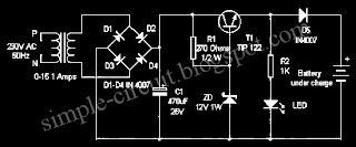
Most of the battery chargers do not have current and voltage regulation provisions. The step down voltage is simply used for charging. These chargers develop internal resistance so the output voltage drops when the battery is connected to the charger. This is a design circuit for the charger circuit. This is the figure of the circuit;
Simple Regulated Charger Circuit schematic with explanation


0-15 1 Ampere step down transformer drops 230 volt AC into 15 volt AC which is rectified through the bridge rectifier comprising D1 through D4. The rectified DC is then made ripple free by C1 and send to the collector of the medium power NPN transistor T1 to give regulated output. Resistor R1 and Zener diode ZD are used for both voltage and current regulation. Output current from the emitter of T1 depends on the value of R1 which can be changed according to the requirement using the ohms law. 12 volt Zener diode gives constant 12 volts to the base of T1 so that output voltage remains 12 volt irrespective of the input fluctuations. Diode D5 is polarity protector that prevents short circuiting if the polarity of the battery is reversed. LED indicates the charging process.

Simple Servo Tester Circuit schematic with explanation

Tags

This is a circuit for a simple servo tester which will comprehensively test the capabilities of almost any modern servo. It has two pushbuttons, CENTRE and SWEEP and a potentiometer. This is the figure of the circuit;

Simple Servo Tester Circuit schematic with explanation

CENTRE Does exactly that, centers the servo, afterwards the potentiometer determines position. SWEEP Sweeps the servo back and forth at a rate determined by the potentiometer setting. The PIC uses its internal timer to set up a constant frame duration of 20ms and the on/off ratio is set by the user.

Simple Ham Radio Circuit For Audio Filter circuit schematic with explanation

Tags


One of the earliest modes of radio communications is the use of Morse Code on a continuous wave carrier (CW) which is interrupted to generate a signal in forming an alphabet. Though it looks simple, this method is often makes less reliable as the surrounding man-made noise and atmospheric noise caused interference to the receiver station. This project will help to filter out the interference signal and ensure that the signal received from the Morse code station stand out. The circuit design of the filter circuit is simple and easy to build. Figure below shows the filter's selectivity response curve. It is sharp at the peak at 20dB at the audio frequency of 800kHz - 900kHz;


It uses common parts that can be purchased easily from any electronic shops. At the core of the circuit is a OP AMP where its input is connected to the headphone jack of the receiver. Some of the amplified signal is feedback through potentiometer VR1 to the non inverting input which helps to boosts the gain and hence called positive feedback. Some is passed to the inverting input through a LC circuit. This cancels the gain of the amplifier except at the resonant frequency - high impedance at resonance state. The amount of positive feedback is adjusted using the potentiometer VR1.

L choke should be in the region of 5H but this is not critical. Try using the winding of an audio transformer to make this choke. The output of this filter is connected to the earphones. On Switch SW and on the radio. Vary the VR1 until it goes into oscillation and then turn it back a bit. Tune across the code station and you will hear a sharp peak response effectively cutting off other noise and interference.

Simple Ni-Cd Battery Discharge Limiter Circuit schematic with explanation

Tags


This is a very simple Ni-cd battery discharge limiter electronic project can be designed like in this circuit diagram using few common electronic parts. This circuit is very simple and can be used in many compact designs. This circuit disconnects the battery from the load when the output voltage falls bellow a preset level. C1 charges through R1 and turns on Q2. This is the figure of the circuit;

Simple Ni-Cd Battery Discharge Limiter Circuit schematic with explanation

Collector current flows through R2 turning Q1 on and battery is connected to the load. When the output voltage falls bellow a point set by RV1, Q2 turns off, Q1 turns off and further discharge of the battery is prevented. The maximum output that can be supported by this discharger circuit is around 3 amperes. At the input you can connect on or two 12 volt Ni-Cd batteries.

Simple Adjustable Sine/Square Wave Oscillator Circuit schematic with explanation

Tags


This is a design circuit for simple easily tuned / adjustable sine and square wave oscillator. This is the figure of the circuit;

Simple Adjustable Sine/Square Wave Oscillator Circuit schematic with explanation

This circuit provides sine and square wave at frequency of below 20Hz up to above 20KHz. The benefit of this circuit diagram is that you can adjust the output frequency by varry the variable resistor of R6.

Simple Electronic Combination Lock Circuit schematic with explanation

Tags


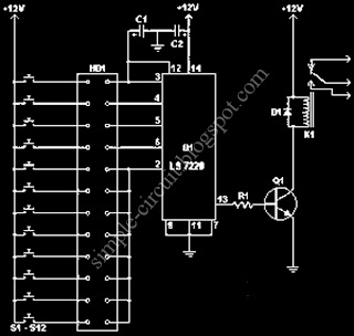
This is a design circuit for a very easy and simple electronic combination lock based on IC LS7220. This could be the circuit diagram of a easy electronic combination lock by using IC LS 7220.This circuit may be applied to activate a relay for controlling (on & off) any device each time a preset combination of 4 digits are pressed. The circuit may be operated from 5V to 12V. This is the figure of the circuit;
Simple Electronic Combination Lock Circuit schematic with explanation

To set the mixture connect the appropriate switches to pin 3,4,5 and 6 of the IC through the header. As an example if S1 is connected to pin 3, S2 to pin 4 , S3 to pin 5, S4 to pin 6 of the IC ,the combination is going to be 1234.This way we can create any 4 digit combinations. Then connect the rest of the switches to pin 2 of IC. This will cause the IC to reset if any invalid key is pressed , and entire key code has to be re entered. When the correct key combination is pressed, then the output ( relay) will be activated for a preset time driven by the capacitor C1.Here, it is set to be 6S.Increase the value of C1 to increase the preset time.

For the keypad, arrange the switches in a 3X4 matrix on a PCB (Printed Circuit Board).Write the digits on the keys by using a marker. Instead of applying numbers I wrote some symbols!.The bad guys is going to be more confused with this.

Component Part List:
· C1 = 1uF 25V
· C2 = 220uF 25V
· R1 = 2.2K Ohm
· Q1 = 2N3904 / 2N2222
· D1 = 1N4148 / 1N4001-1N4007
· K1 = 12V SPDT Relay / Any appropriate relay with 12V coil
· U1 = LS7220 Digital Lock IC
· S1-S12 = SPST Momentary Pushbutton Keypad (see notes)
· HD1 = 12 Position Header

Infrared Modulation Identifier Circuit schematic with explanation

Tags


This is a design circuit for Infrared Modulation Identifier using remote control. Here’s the figure of the circuit;
Infrared Modulation Identifier Circuit schematic with explanation

In this circuit illustrates how the modulated carrier of infrared is measured by displaying the waveform on a frequency counter after the signal received is amplified.

LM3909 based Simple LED Flasher Circuit schematic with explnation

Tags
This is a very -very easy and simple LED flasher circuit with only needs three components that are: a flasher IC, a LED and an electrolytic capacitor. Here’s the figure of the circuit;

Component list:
LED1_________Red LED
C1___________100uf/16V
IC1__________LM3909

Simple Galvanometer Circuit schematic with explanation

Tags


This circuit is design for galvanometer circuit. According to Wikipedia.org, a galvanometer is an analog electromechanical transducer to be used for detecting and measuring electric current (ammeter). In this circuit design, the voltage across Rm and Rv is the same because they are in parallel. The resistor Rv is a variable resistor. Here’s the figure of the circuit;

Simple Galvanometer Circuit schematic with explanation

Simple Positive (+) to Negative (-) Voltage Inverter Circuit

Tags


This is a simple circuit that can be used to convert the positive input voltage become negative voltage. Here’s the figure of the circuit;

Simple Positive (+) to Negative (-) Voltage Inverter Circuit

Component list:

Part Total Qty. Description
R1 1 24K 1/4 Watt Resistor
R2 1 56K 1/4 Watt Resistor
C1 1 3300pF 25V Ceramic Capacitor
C2 1 47uF 25V Electrolytic Capacitor
C3 1 10uF 25V Electrolytic Capacitor
D1, D2 2 1N4148 Silicon Diode
U1 1 555 Timer
MISC 1 Wire, Board

In this circuit, V+ can be anywhere from 4 to 16V. -V is one volt less than V+. So, for -12V output, use +13V input. The maximum current output of the circuit is about 280mA, more than enough for a few op amps. For better regulation, a 79LOxx series regulator can be used. A zener diode may also be used to regulate the output voltage.

Advertisement