Six-LED Bar Power Indicator Circuit Schematic With Explnation

Tags


Six-LED Bar Power Indicator Circuit Schematic With Explnation
This device, connected to the loudspeaker output of an audio amplifier, will indicate the instantaneous output power delivered to the loudspeaker(s) by means of six LEDs illuminating one after another by voltage values increasing little by little, providing the visual impression of a luminous bar or column, increasing and decreasing in height following the increase and decrease of the signal's level.The input signal is first rectified by D1 and then sent to six different voltage dividers, one for each LED. In this way, the indication provided by the LEDs illumination of this "Power Display", will be related to the instantaneous power sunk by the whole loudspeaker cabinet.Six output power levels are displayed by the LEDs in a 2W - 80W range (no setup required). Each nominal power level indication into 8 Ohms load is reached when the respective LED illuminates at full brightness.


Six-LED Bar Power Indicator


Parts:


R1_____________220R 1/2W Resistor
R2,R5,R6,R8____100R 1/4W Resistors
R10,R12,R14____100R 1/4W Resistors
R3_____________220R 1/4W Resistor
R4,R7__________330R 1/2W Resistors
R9_____________560R 1/2W Resistor
R11____________820R 1/2W Resistor
R13______________1K2 1/2W Resistor
D1___________1N4004 400V 1A Diode
D2,D4,D6__BZX79C2V7 2.7V 500mW Zener Diodes D3,D5,D7,D8,D9,D10 Red LEDs (Any dimension and shape) (See Notes)


Notes:


The output power indicated by each LED must be doubled when 4 Ohms loads are driven. * The circuit can be adapted to suit less powerful amplifiers by reducing the number of LEDs and related voltage dividers. * LEDs of any dimension can be used, but rectangular shaped devices will be more suitable to be compacted in bars or columns. * For a stereo amplifier, two identical circuits are required.

Versatile FM Transmitter Circuit Schematic With Explnation


Versatile FM Transmitter Circuit Schematic With Explnation
Here is the circuit diagram of a versatile FM transmitter that doesn’t have a coil. The circuit is simple and easy to assemble.


fm-transmitter-without-coil.JPG


The gate N1 acts as a buffer for strengthening the signals from the condenser microphone. The inverter N2 with its associated components forms a radio frequency oscillator in the FM region.The varicap diode BB109 is used for frequency modulating the audio signal to the carrier wave generated by the oscillator.Inverters N4 t0 N6 are used to drive the antenna.As the N4,N5,N6 are connected in parallel their effective output impedance is very less and can easily drive the antenna.


Notes.

* All electrolytic capacitors must be rated 10V.
* Use any general purpose condenser microphone.You can easily get one from old telephone or tape recorder.
* Use a 10 cm long wire as antenna.
* Gates N1 to N6 belong to same IC CD4069.
* The battery can be a 9V transistor radio battery.Adapters are not recommended because they would induce noise in the circuit.

Long range AM transmitter Circuit Schematic With Explnation


Long range AM transmitter Circuit Schematic With Explnation
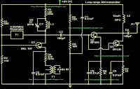
This is a long range transmitter.This circuit can send signals up to 2km.So that you have to use 1m copper wire.The power of this transmitter has been increased by usin two transistors. When you use this transmitter do give power with out connecting the antenna.Because it will burn your transistors.


Long range AM transmitter Circuit Schematic With Explnation


Note


# The transformer T1 can be a general purpose audio driver transformer seen in transistor radios.

# The inductor L1 can be made by making 56 turns of 365 WG enameled copper wire on a 1 cm former.

# Inductor L2 can be a 10 mH general purpose radio frequency choke.

# The circuit can be powered from a 9V PP3 battery.

Digital Volume Control Circuit Schematic With Explnation


Digital Volume Control Circuit Schematic With Explnation
This circuit could be used for replacing your manual volume control in a stereo amplifier. In this circuit, push-to-on switch SW1 controls the forward (volume increase) operation of both channels while a similar switch SW2 controls reverse (volume decrease) operation of both channels. A readily available IC from Dallas semiconductor, DS1669 is used here.


Digital Volume Control Circuit Schematic With Explnation

Parts:

J1 = RCA Audio Input Socket J2 = RCA Audio Input Socket C1 = 0.1uF-16V Ceramic Disc Capacitor C2 = 0.1uF-16V Ceramic Disc Capacitor C3 = 0.1uF-16V Ceramic Disc Capacitor IC1 = DS1669 (is available from Dallas SCo. SW1 = Momentary Push Button Switch SW1 = Momentary Push Button Switch

Notes:


* Replaces mechanical variable resistors. * Electronic interface provided for digital as well as manual control. * Wide differential input voltage range between 4.5 and 8 volts. * Wiper position is maintained in the absence of power. * Low-cost alternative to mechanical controls. * Applications include volume, tone, contrast, brightness, and dimmer control. * The circuit is extremely simple and compact requiring very few external components. * The power supply can vary from 4.5V to 8V. * The input signal should not fall below -0.2 volts.

Spy FM Transmitter Circuit Schematic With Explnation


Spy FM Transmitter Circuit Schematic With Explnation
This is so impotent circuit for us,Because we can use this circuit as a spy unit.This circuit can transmit signals about 30m.And the other important thing is the power of this circuit we can operate this circuit with 1.5v to 3v(1.8 mA at 1.5 Volts )


Spy FM Transmitter Circuit Schematic With ExplnationNote

# If you are unable to find the transistor here use these transistors Because here you can use equal transistors such as 2N2222A, BFxxx series, BC109B, C, and even well known BC238.

# Use 1.5v to 3v for this circuit.Don't supply more than 3v(3v can cover the max range 30m)

Melody Generator using IC UM66 Circuit Schematic With Explnation


Here is the simplest melody generator circuit you can make using an IC.The UM66 series are CMOS IC’s designed for using in calling bell, phone and toys. It has a built in ROM programmed for playing music. The device has very low power consumption.Thanks for the CMOS technology.The melody will be available at pin3 of UM66 and here it is amplified by using Q1 to drive the speaker.Resistor R1 limits the base current of Q1 within the safe values.Capacitor C1 is meant for noise suppression.


http://www.circuitstoday.com/wp-content/uploads/2008/02/melody.JPG


http://www.circuitstoday.com/wp-content/uploads/2008/02/um66.JPG


Notes

* Power supply must be between 1.5V & 4.5V .Do not exceed 4.5 V.
* Speaker can be driven with external NPN transistor.
* Melody begins from the first note if power is reseted.
* Assemble the circuit on a good quality common board.
* If transistor HE8050S is not available use any NPN transistor like BC548 or 2N2222.

VHF field strength meter Circuit Schematic With Explnation

Tags


VHF field strength meter Circuit Schematic With Explnation
This is a simple and low cost wide band VHF field strength meter. The field strength is measured by converting the radio signal to DC and measuring it.


VHF field strength meter Circuit Schematic With Explnation


The RF signal will be picked up by the coil and rectified by the diode D1.Even a very small DC voltage is sufficient to alter the biasing of FET and it will be reflected in the meter as an indication of the presence of a radio signal. The meter can be calibrated by adjusting the preset R2 to make meter M1 read ZERO in the absence of any radio signal. This circuit is not very sensitive, but can sense radio signals from hand held FM transmitters up to a distance of few meters( ideal for theoretical demonstrations).


Notes.

* The circuit can be assembled on a general purpose PCB.
* Use a 9V PP3 battery for powering the circuit.
* Use a 250uA FSD current meter for M1.Using a lower FSD meter will improve sensitivity.
* The coil L1 can be made by making 6 turns of 20 SWG enameled copper wire on a inch plastic former.
* The antenna can be a telescopic whip antenna.

FM Radio Jammer circuit diagram Circuit Schematic With Explnation

Tags

FM Radio Jammer circuit diagram Circuit Schematic With Explnation

FM Radio Jammer circuit diagram Circuit Schematic With Explnation
This is FM radio jammer circuit diagram.This is not legal device in many countries.So dont misuse this.we dont get any response of it.

FM Radio Jammer circuit diagram Circuit Schematic With Explnation


Note

# This circuit operates with 9V

# L1 make 6 turns of 16AWG enamelled copper wire on a 9mm plastic former.

Ding-Dong sound generator Circuit Schematic With Explnation


Ding-Dong sound generator Circuit Schematic With Explnation
This is the circuit diagram of a ding dong sound generator based on two NE555 timer ICs.The circuit is designed to toggle between two adjustable frequencies to produce the ding dong sound. The first NE555 (IC1) is wires as an astable multivibrator operating at 1Hz. The frequency of the second NE555 (IC2) is modulated by the output from the first IC. This is attained by connecting the output of first IC to the control pin (pin5) of the second IC. The tone of the sound depends on the frequency of the second IC and the changeover time depends on the frequency of the first IC.


Notes.

* The circuit can be assembled on a Vero board.
* Use 9V PP3 battery for powering the circuit.
* POT R4 can be used to adjust the tone of the sound.
* POT R2 can be used to adjust the change over time.
* IC1 and IC2 must be mounted on holders.
* K1 can be a 8 ohms, 1/2 watt tweeter

FM Transmitter circuit diagram (50M) Circuit Schematic With Explnation

Tags

FM Transmitter circuit diagram (50M) Circuit Schematic With Explnation

FM Transmitter circuit diagram (50M) Circuit Schematic With Explnation
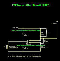
This is FM transmitter circuit diagram.By using this circuit diagram you can send signals up to 50M.Here I have used 2N2222 Transistor.This circuit can be operated with 3V

FM Transmitter circuit diagram (50M) Circuit Schematic With Explnation

Note

# L1= 5 turns of 24AWG wire on a 1cm plastic former.

# Antenna can be a 25cm long 18AWG wire.

Two transistor siren Circuit Schematic With Explnation


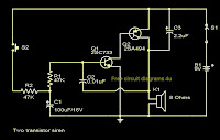
Here is the circuit diagram of a simple two transistor alarm circuit that can be operated from a 9V PP3 battery. Here the two transistors are wired to form an oscillator whose frequency increases when switch S2 is pressed and decreases when S2 is released. In order to attain this the base of Q1 is biased from an RC circuit comprising of R2 and C1.When S2 is pressed C1 is charged through the resistor R2.As the voltage across the C1 increases the time constant decreases and this results in an increases in the frequency. When S2 is released capacitor discharges and the frequency of the tone decreases. The sound heard from the speaker will be almost like that of a siren.

Two transistor siren Circuit Schematic With Explnation


Notes.

* The circuit can be assembled on a Vero board.
* Use a 9V PP3 battery for powering the circuit.
* Switch S2 can be a miniature push button switch.
* The type no of transistors are not very significant here.

5 to 500 feet transmitter Circuit Schematic With Explnation


5 to 500 feet transmitter Circuit Schematic With Explnation
This is so useful circuit because this circuit can transmit signals 5 feet to 500 feet.Here I have used common transistor 2N5225 If you are unable to find this you can use any general purpose transistor.

5 to 500 feet transmitter Circuit Schematic With Explnation

Note

# About L1 is mentioned on the picture

# This circuit operates with 9V DC

# use 5cm wire as an antenna

Whistle to beep Circuit Schematic With Explnation


This simple circuit produces a beeping sound that lasts for around 3 seconds whenever you make a whistle. The CMOS Hex inverter CD4049 is the heart of this circuit. Out of the six inverters in CD4049, U1a is wired as an audio amplifier which amplifies the signal picked up by the microphone M1.The U1b is wired as a band pass filter with center frequency around 2KHz.The filter is necessary in order to pass the frequency corresponding to whistling sound and suppress all other frequencies .If the filter is not there, the circuit could easily get false triggered.U1d is wired as a 3S delay monostable multivibrator.The output U1d drives the astable multivibrator formed by U1e and U1f.The astable multivibrator is operating around 4Hz.The combined effect is a intermittent beeping sound that lasts for around 3S.Transistor Q1 is used to drive the buzzer B1.


Notes.

* Assemble the circuit on a good quality PCB.
* The circuit can be powered from a 3V battery.
* IC U1 is a CMOS CD4049 Hex inverter.
* M1 can be an electret microphone.
* B1 can be a 3V piezo buzzer.
* Mount the IC on a holder.
* The duration of beeping can be adjusted by varying the components C4 and R9.

Simple radio Circuit Schematic With Explnation


Simple radio  Circuit Schematic With Explnation

some persons asked simple radio circuit diagrams.Here you can see very simple circuit diagram.When I tested this my first time I enjoyed very much.When the signals are coming you can here some sounds like ne ne nee nic nee nee nee nee.so test this and enjoy.


Simple radio  Circuit Schematic With Explnation


Note:

# Don't use more than 4.5V

# Build this on a pcb

#If the signals don't come move the main coil here and there then you can here some sounds.

# Firstly this circuit was designed by Elmer G. Osterhoudt in the early 30's

Canary chirp generator Circuit Schematic With Explnation

Tags


This is a simple electronic alarm circuit that imitates the chirping of a canary. The circuit is nothing but a Hartley oscillator with few more passive components added. As the capacitor C1 charges through the resistor R1 and the transistor Q1 is driven to cut off. This makes the oscillations to stop. As the capacitor discharges through the Resistor R1 and base emitter junction of the transistor the oscillation start again. Actually the R1 and C1 are the components that make the characteristic chirping sound.


Notes.

* Assemble the circuit on a general purpose PCB.
* The circuit can be powered from a 9V PP3 battery.
* The transformer T1 can be a audio output transformer like LT700.
* If LT700 is not available, try the audio output transformer used on you old transistor radio board.
* The speaker can be an 8 ohm tweeter.
* Switch S1 can be a push button switch.
* The chirping sound can be altered by changing the value of R1 and C1.

5 band graphic equalizer using a single IC Circuit Schematic With Explnation

Tags


5 band graphic equalizer using a single IC Circuit Schematic With Explnation

This circuit uses a single chip, IC BA3812L for realizing a 5 band graphic equalizer for use in hi-fi audio systems.
The BA3812L is a five-point graphic equalizer that has all the required functions integrated onto one IC. The IC is comprised of the five tone control circuits and input and output buffer amplifiers. The BA3812L features low distortion, low noise, and wide dynamic range, and is an ideal choice for Hi-Fi stereo applica-tions. It also has a wide operating voltage range (3.5V to 16V), which means that it can be adapted for use with most types of stereo equipment.


5 band graphic equalizer using a single IC Circuit Schematic With Explnation


The five center frequencies are independently set using external capacitors, and as the output stage buffer amplifier and tone control section are independent circuits, fine control over a part of the frequency bandwidth is possible, By using two BA3812Ls, it is possible to construct a 10-point graphic equalizer. The amount of boost and cut can be set by external components. The recommended power supply is 8V, but the circuit should work for a supply of 9V also. The maximum voltage limit is 16V. The circuit given in the diagram operates around the five frequency bands: * 100Hz * 300Hz * 1kHz * 3kHz * 10kHz

Touch Musical Bell Circuit Schematic With Explnation


According to the present situation People are used to use various types of electrical equipments.So I thought to give you a very useful circuit.This is a Touch musical bell circuit diagram.When you just touch TP(touch plate)The circuit will activate.Here I have used very common IC UM 3481.


Note

# use 2W 8 ohm speaker
# This circuit can be operated with 3V power supply

40 MHz Wideband RF Amplifier Circuit Schematic With Explnation


40 MHz Wideband RF Amplifier Circuit Schematic With Explnation

This transmitter works, radio frequency range with a wideband frequency of 40 MHz.So you can use this with lots of electrical equipments


40 MHz Wideband RF Amplifier Circuit Schematic With Explnation


The circuit is consuming a total of 7 mA of current while the gain is in the measurement of 20 dB. All these values are due to the presence of a 12 V up to 15 V DC supply. The input and the output of the circuit are designed to be compatible with coaxial cables with complex resistance of 75 Ohms.


Part List

R1=75ohm
R2=10Kohm
R3-7=5.6Kohm
R4-5 =4.7Kohm
R6=820ohm
R8=470ohm
R9=2.2Kohm
R10=68ohm
C1-3=47nF 100V
C2-4=10nF 100V
C5-6=47nF 100V
Q1-2-3=AF125
J1-2=Jack BNC

Simple Melody Generator Circuit Schematic With Explnation


This is so impotent circuit for you all.On the other hand this is so important circuit for beginners.Here I have used IC UM66 You can get various musics when you buy UM66 with different numbers.


Note:

# Don't supply more than 3V

# Build this circuit on a pcb

Three sirens in one Circuit schematic with explanation

Tags

Three sirens in one Circuit schematic with explanation


This is a siren circuit diagram Here I have used UM3561 circuit diagram.This circuit can be operated with 3V.It can generate 3 sirens.Here I have used IC 2SC9013 you can use the same IC or similar IC. Use 8ohm 0.2W speaker.


Note:-

* Don't use more than 3V
* Don't use this for unnecessary things
* Build this circuit on a PCB

AM receiver Circuit Schematic With Explnation

Tags


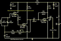
Here is a low cost AM receiver circuit that can be tuned from around 550 to 1100 KHz. Three transistors are used in this project. The transistors Q1 and Q2 are wired as a compound transistor pair in which Q1 is an emitter follower and Q2 is a common emitter amplifier. The emitter follower prevents the loading of tank circuit, while the common emitter amplifier necessary voltage gain. The L1 and C2 forms the tank circuit.The L1 also does the job of antenna.The series combination of R6 and R7 gives a regenerative feedback between output of the Q2 and tank circuit. The transistor Q3 performs the demodulation of the carrier signal. It also provides amplification the demodulated signal. The audio output is coupled out from the collector of Q3 via the capacitor C3.Capacitor C6 provides some noise filtering.

Circuit Schematic With Explnation


Notes.

* The circuit can be assembled on a general purpose PCB.
* Use a 9V PP3 battery for powering the circuit.
* R7 can be used to adjust the sensitivity and selectivity of the circuit.
* A high impedance head phone can be used for listening the radio.
* For L1 make 60 turns of 26 SWG enameled copper wire on a 3/8 inch diameter, 3inch long ferrite rod.
* The moving plates of C2 must be connected to the base of Q1 and fixed plates must be connected to the junction of C3 and R6.Reversing the connection may decrease the stability.

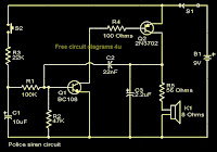
Police siren Circuit Schematic With Explnation


Circuit Schematic With Explnation
The circuit given here produces an alarm similar to the police siren. When you press the push button switch S2 capacitor C1 will charge and this will make the transistor Q1 to ON slowly. When the switch S1 is released the C1 will discharge and the transistor Q1 will become OFF slowly. When the Q1 is switched ON, its collector voltage falls and makes the transistor Q2 ON. The capacitor C2 will be charged almost to full supply voltage. This results in an increase in the collector-emitter voltage of Q2.This change in voltage is coupled to the base of Q1 via the capacitor C2.As a result the transistor Q1 comes slightly out of saturation. As a result the collector voltage of Q1 drops and makes the Q2 more OFF. This action continues until both transistors become OFF. Then the capacitor C2 discharges, and transistor Q1 will be switched ON again to start a new cycle. When the capacitor C1 is charged the tone will rise and when the capacitor C1 is discharging the tone will fall.


Circuit Schematic With Explnation


Notes.

* The circuit can be assembled on a vero board.
* The circuit can be powered from 9V DC.
* Switch S1 can be used as a power ON/OFF switch.
* K1 can be an 8 Ohm loud speaker.

Basic Sound Generator Circuit Schematic with explanation

Basic Sound Generator Circuit Schematic with explanation


This is so important circuit for the persons who came to this field recently.Here I have used common IC NE555.According to the pules (Frequency) of the IC We can generate the sound.You can change the speed of the sound by adjusting R2.This circuit operates with 5V.


# Note

# Don't give over 5V
# Build this circuit on a PCB
# Don't give the much heat to the IC NE555

Advertisement