Build a 300 Watt Subwoofer Power Amplifier Circuit Diagram


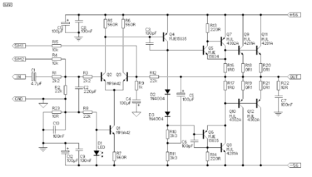
The output devices are MJL4281A (NPN) and MJL4302A (PNP), and feature high bandwidth, excellent SOA (safe operating area), high linearity and high gain. Driver transistors are MJE15034 (NPN) and MJE15035 (PNP). All devices are rated at 350V, with the power transistors having a 230W dissipation and the drivers are 50W.

Having built a P68 using these transistors, I recommend them highly - the amplifier is most certainly at its very best with the high gain and linearity afforded by these devices. Note that there are a few minor changes to the circuit (shown below).

High power amps are not too common as projects, since they are by their nature normally difficult to build, and are expensive. A small error during assembly means that you start again - this can get very costly. I recommend that you use the PCB for this amplifier, as it will save you much grief. This is not an amp for beginners working with Veroboard!

The amplifier can be assembled by a reasonably experienced hobbyist in about three hours. The metalwork will take somewhat longer, and this is especially true for the high continuous power variant. Even so, it is simple to build, compact, relatively inexpensive, and provides a level of performance that will satisfy most requirements.

300W Sub woofer Power Amplifier Circuit Diagram

Build a 300 Watt Subwoofer Power Amplifier Circuit Diagram

Fig 1
WARNINGS:
  • This amplifier is not trivial, despite its small size and apparent simplicity. The total DC is over 110V, and can kill you.
  • The power dissipated is such that great care is needed with transistor mounting.
  • The S300 is intended for intermittent duty on 4 Ohm loads, as will normally be found in a subwoofer. It is NOT intended for PA or any other continuous duty, and although it may work fine for may years, I absolutely do not recommend this.
  • For continuous duty, do not use less than 8 Ohms.
  • There is NO SHORT CIRCUIT PROTECTION. The amp is designed to be used within a subwoofer enclosure, so this has not been included. A short on the output will almost certainly destroy the amplifier.
DO NOT ATTEMPT THIS AMPLIFIER AS YOUR FIRST PROJECT

Please note that this amp is NOT designed for continuous high power into 4 Ohms. It is designed for intermittent duty, suitable for an equalized sub woofer system (for example using the ELF principle - see the Project Page for the info on this circuit). Where continuous high power is required, another 4 output transistors are needed, wired in the same way as Q9, Q10, Q11 and Q12, and using 0.1 ohm emitter resistors.

Continuous power into 8 ohms is typically over 150W, and it can be used in the form shown at full power into an 8 ohm load all day, every day. The additional transistors are only needed if you want to do the same thing into 4 ohms!

The circuit is shown in Figure 1, and it is a reasonably conventional design. Connections are provided for the Internal SIM (published elsewhere on the Project Pages), and filtering is provided for RF protection (R1, C2). The input is via a 4.7uF bipolar cap, as this provides lots of capacitance in a small size. Because of the impedance, little or no degradation of sound will be apparent. A polyester cap may be used if you prefer - 1uF with the nominal 22k input impedance will give a -3dB frequency of 7.2Hz, which is quite low enough for any sub.
The input stage is a conventional long-tailed pair, and uses a current sink (Q1) in the emitter circuit. I elected to use a current sink here to ensure that the amp would stabilise quickly upon application (and removal) of power, to eliminate the dreaded turn on "thump". The amp is actually at reasonably stable operating conditions with as little as +/-5 volts! Note also that there are connections for the SIM (Sound Impairment Monitor), which will indicate clipping better than any conventional clipping indicator circuit. See the Project Pages for details on making a SIM circuit.
The Class-A driver is again conventional, and uses a Miller stabilisation cap. This component should be either a 500V ceramic or a polystyrene device for best linearity. The collector load uses the bootstrap principle rather than an active current sink, as this is cheaper and very reliable (besides, I like the bootstrap principle :-)

All three driver transistors must be on a heatsink, and D2 and D3 should be in good thermal contact with the driver heatsink. Neglect to do this and the result will be thermal runaway, and the amp will fail.

C11 does not exist on this schematic, so don't bother looking for it. It was "mislaid" when the schematic was prepared, and I didn't notice until someone asked me where and what it was supposed to be. Sorry about that.
It is in the output stage that the power capability of this amp is revealed. The main output is similar to many of my other designs, but with a higher value than normal for the "emitter" resistors (R16, R17). The voltage across these resistors is then used to provide base current for the main output devices, which operate in full Class-B. In some respects, this is a "poor-man's" version of the famous Quad "current dumping" circuit, but without the refinements.

Although I have shown MJL4281A and MJL4302A output transistors, because they are new most constructors will find that these are not as easy to get as they should be. The alternatives are MJL21193/ MJL21194
Build a 300 Watt Subwoofer Power Amplifier Circuit Diagram
Fig 2

Note: It is no longer possible to recommend any Toshiba transistors, since they are the most commonly counterfeited of all. The 2SA1302 and 2SC3281 are now obsolete - if you do find them, they are almost certainly fakes, since Toshiba has not made these devices since around 1999~2000.

Use a standard green LED. Do not use high brightness or other colors, as they may have a slightly different forward voltage, and this will change the current sink's operation - this may be a miniature type if desired. The resistors are all 1/4W (preferably metal film), except for R10, R11 and R22, which are 1W carbon film types. All low value resistors (1 ohm and 0.1 ohm) are 5W wire wound types.

Because this amp operates in "pure" Class-B (something of a contradiction of terms, I think), the high frequency distortion will be relatively high, and is unsuited to high power hi-fi. At the low frequency end of the spectrum, there is lots of negative feedback, and distortion is actually rather good, at about 0.04% up to 1kHz.

Power output into 4 ohms is over 250W continuous, and for transients exceeds 300W easily. Use of a big power transformer and massive filter caps will allow the amp to deliver close to 350W continuous, but if you really want to use it like that, I very strongly recommend the additional output transistors (see above comments on this topic).

Power Dissipation Considerations
I have made a lot of noise about not using this amp for continuous duty into 4 ohms without the extra transistors. A quick calculation reveals that at the worst case, the output and transistor voltage will be the same - i.e. at 28V. With 28V, load (and transistor) current is 7A, so the instantaneous dissipation is therefore 28 * 7 = 196W. This means that the four final transistors do most of the work, with the others having a relatively restful time.

Since I like to be conservative, I will assume that they contribute no more than about 1.5A (which is about right). This means that they only dissipate 48W, with the main O/P devices dissipating a peak of 74W each. The specified transistors are 130W, and the alternatives are 150W, so where is the problem?

The problem is simple - the rated dissipation for a transistor is with a case temperature of 25°C. As the amp is used, each internal transistor die gets hot, as does the transistor case - the standard derating curves must be applied. Add to this the reactive component as the loudspeaker drives current back into the amp, and it becomes all too easy to exceed the device dissipation limits.

Figure 1A shows the doubled output stage, with Q9, Q10, Q11 and Q12 simply repeated - along with the emitter resistors. Each 1/2 stage has its own zobel network and bypass caps as shown, as this is the arrangement if the dual PCB version is built. When you have this many power transistors, the amp will happily drive a 4 ohm load all day - with a big enough heatsink, and / or forced cooling (highly recommended, by the way).

A Few Specs and Measurements

The following figures are all relative to an output power of 225W into 4 ohms, or 30V RMS at 1kHz, unless otherwise stated. Noise and distortion figures are unweighted, and are measured at full bandwidth. Measurements were taken using a 300VA transformer, with 6,800uF filter caps. Mains voltage was about 4% low when I did the tests, so power output will normally be slightly higher than shown here if the mains are at the correct nominal voltage.

Gain27dB
Power (Continuous)240W (4 ohms)

153W (8 ohms)
Peak Power - 5 ms185W (8 ohms)
Peak Power - 10 ms172W (8 ohms)
Input Voltage1.3V RMS
Noise-63dBV (ref. 1V)
S/N Ratio92dB
Distortion0.4%
Distortion (@ 4W)0.04% (1 Khz)
Distortion (@ 4W)0.07% (10 kHz)
Slew Rate> 3V/us
Power Bandwidth30 kHz
These figures are quite respectable, especially considering the design intent for this amp. While it would not be really suitable for normal hi-fi, even there it is doubtful that any deficiencies would be readily apparent, except perhaps at frequencies above 10kHz. While the amp is certainly fast enough (and yes, 3V/us actually is fast enough - full power is available up to 30kHz), the distortion will be a bit too high.

Note that the "peak power" ratings represent the maximum power before the filter caps discharge and the supply voltage collapses. I measured these at 5 milliseconds and 10 milliseconds. Performance into 4 ohm loads will not be quite as good, as the caps will discharge faster. The supply voltage with zero power measured exactly 56V, and collapsed to 50.7V at full power into 8 ohms, and 47.5V at full power into 4 ohms.

Photo of amp
Photo of Completed Prototype

The photo does not show the silk screened component overlay, since this is the prototype board. The final boards have the overlay (as do all my other boards).

As can be seen, this is the single board version. The driver transistors are in a row, so that a single sheet aluminium heatsink can be used for all three. Holes are provided on the board so the driver heatsink can be mounted firmly, to prevent the transistor leads breaking due to vibration. This is especially important if the amp is used for a powered subwoofer, but will probably not be needed for a chassis mounted system.
The driver and main heatsinks shown are adequate for up to 200W into 4 ohms with normal program material. The power transistors are all mounted underneath the board, and the mounting screw heads can be seen on the top of the board.

Deceptively simple, isn't it?

Power Supply

WARNING: Mains wiring must be performed by a qualified electrician - Do not attempt the power supply unless suitably qualified. Faulty or incorrect mains wiring may result in death or serious injury.
The basic power supply is shown in Figure 2. It is completely conventional in all respects. Use a 40-0-40 V transformer, rated at 300VA for normal use. For maximum continuous power, a 500VA or bigger transformer will be needed. This will give a continuous power of about 350W, and peak power of close to 400W is possible with a good transformer. Remember my warnings about using the amp in this way, and the need for the additional output transistors.

Build a 300 Watt Subwoofer Power Amplifier Circuit Diagram
Figure 2 - Basic Power Supply Circuit
For 115V countries, the fuse should be 6A, and in all cases a slow blow fuse is required because of the inrush current of the transformer.

C1 must be rated for 240V AC (or 120V AC) operation - do not use standard 250V DC caps under any circumstance, as they will fail, and R1 will explode! This is not intended as humour - this is fact! C1 and R1 may be omitted in most cases, and if you cannot get a mains rated capacitor I suggest that you don't install these components.

The supply voltage can be expected to be higher than that quoted at no load, and less at full load. This is entirely normal, and is due to the regulation of the transformer. In some cases, it will not be possible to obtain the rated power if the transformer is not adequately rated.

Bridge rectifiers should be 35A types, and filter capacitors must be rated at a minimum of 63V. Wiring needs to be heavy gauge, and the DC must be taken from the capacitors - not from the bridge rectifier.

Although shown with 4,700uF filter capacitors, larger ones may be used. Anything beyond 10,000uF is too expensive, and will not improve performance to any worthwhile degree. Probably the best is to use two 4,700uF caps per side (four in all). This will actually work better than a single 10,000uF device, and will be cheaper as well.

NOTE: It is essential that fuses are used for the power supply. While they will not stop the amp from failing (no fuse ever does), they will prevent catastrophic damage that would result from not protecting the circuit from over-current conditions. Fuses can be mounted in fuseholders or can be inline types. The latter are preferred, as the supply leads can be kept as short as possible. Access from outside the chassis is not needed - if the fuses blow, the amplifier is almost certainly damaged.
Build a 250 to 5000 watts PWM DC/AC 220V Power Inverter Circuit Schemati With explanation


Build a 250 to 5000 watts PWM DC/AC 220V Power Inverter


Build a 250 to 5000 watts PWM DC/AC 220V Power Inverter Circuit Schemati With explanation

Build a 250 to 5000 watts PWM DC/AC 220V Power Inverter Circuit Schemati With explanation

Build a 250 to 5000 watts PWM DC/AC 220V Power Inverter Circuit Schemati With explanation


Build a 250 to 5000 watts PWM DC/AC 220V Power Inverter Circuit Schemati With explanation


Build a 250 to 5000 watts PWM DC/AC 220V Power Inverter Circuit Schemati With explanation


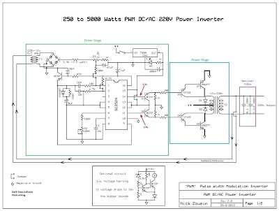
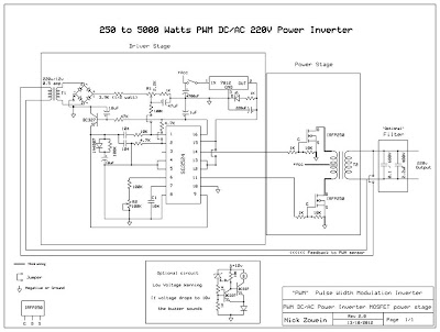
This is my schematic design of a Pulse Width Modulator DC/AC inverter using the chip SG3524 .
I have built this design and using it as a backup to power up all my house when outages occur.

If you like my work and intend to build the circuit don't forget to give me the 5 satrs :D and subscribe to me by clicking on the "follow" button so I know how many people benefit from the design, Thanks

Notes:

>The schematic circuit design is for a 250 watt output, while the pics are of my 1500 watts inverter that i built, to increase the power of the circuit you have to add more of the Q7 and Q8 transistors in parallel, each pair you add will increase your power by 250 watts, ex: to get 750 watts of power from the inverter you need to add in parallel 2 of Q7 and 2 of Q8 to the original design.

>If you increase the power transistors you have to enlarge the T2 transformer to match the new needs, the circuit's transformer is rated 25 amps to handle 250 watts of 220v, for every 1 additional amp you need on the 220v side you have to increase 10 amps on the 12v side, of course there are limits to the thickness of the winding so if you need more than 750 watts i recommend that you use a 24VDC supply instead of 12 volts:

DC voltage and Transformer "T2" winding recommendation:
Power Supply Winding
750w 12VDC P:24V "12-0-12" / S:220V
1500w 24VDC P:48V "24-0-24" / S:220V
2250w 36VDC P:72V "36-0-36" / S:220V
3000w 48VDC P:96V "48-0-48" / S:220V
3750w 60VDC P:120V "60-0-60" / S:220V
4500w 72VDC P:144V "72-0-72" / S:220V
5250w 84VDC P:168V "84-0-84" / S:220V
*The transformer should be "center tapped" at the primary side.
**You can make the secondary 110v if needed.
***The transformer in the pic is a custom made (48V center tapped / 220v ) 2000 watts, weights like 10 kilos.

>R1 is to set the PWM duty cycle to 220v. Connect voltmeter to the output of your inverter and vary VR1 till the voltage reads 220V.

>R2 is to set the frequency to 50 or 60 Hz (R2 range is between 40Hz to 75Hz), so guys that do not have a frequency meter are advised to blindly put this variable resistor mid-way which should drop you in the range of 50~60 Hz.
If you want you can substitue the variable resistor with a fixed resistor using the following formula: F = 1.3 / (RxC)
in our case to get a 50Hz output we remove both the 100K and the variable 100K both from pin 6 and we put instead a 260K fixed resistor and we leave the 0.1uF (the 104 cap) as it is, this change should give out a fixed 50Hz as per the formula :
1.3 / (260,000 ohm x 0.0000001 farad) = 50Hz
But in reality it will not exactly give 50Hz because the 260K resistor has a specific error value margin so does the capacitor, that's why i recommend a variable resistor so that accurate calibration can be achieved.

>Use either tantalum or polyester film "as in pic" for the 104 caps, ceramic disc caps change value once hot and this in turn changes the frequency of the inverter so they are not recommended.

>Pin 10 of the SG3524 can be used to auto shut down the inverter, once a positive voltage is given instead of negative to pin10, the SG3524 will stop oscillating. This is useful for persons wanting to add some cosmetic makeup to their inverters like overload cutoff, low battery cutoff or overheating cutoff.

>Wiring connections on the power stage side should be thick enough to handle the huge amps drain from the batteries. I marked them with dark black on the schema also I included a pic so you see how thick those wires must be.

>The design does not include a battery charger since each person will be building a custom version of the inverter with specific power needs. If you are ordering a custom made transformer you can ask them to take out for you an additional output wire on the primary side to give 14v (between point 0 and this new wire) and use it to charge a 12v battery, of course this needs a seperate circuit to control charging auto cut-off. But anyway this is not advisable because it will shorten the life of the transformer itself since using it as a charger will toast the enamel coating layer of the copper wires over time. Anyway .. YES can be done to reduce cost.

>A cooling fan will be needed to reduce heat off the heat sinks and transformer, i recommend getting a 220v fan and connecting it to the output T2 transformer, when you power up the circuit the fan will start this will always give you a simple way to know that 220v is present and everything is OK.. You can use a computer's old power supply fan if you like.
Note that the fan must suck air out from the inverter case and NOT blow inside, so install it the correct way or it will be useless.
Also note how I fixed both the heat sinks and where the fan is, in a way that the fan sucks hot air from like a channel between the 2 heatsinks.

>2 circuit breakers are recommended instead of fuses, one on the DC side and one on the AC side, depending on your design
Ex: for a 24vDC ( 1500 watts design ) put a 60Amp breaker on the DC side and a 6Amp on the AC side.
For every 1amp of 220vAC you will be draining like 8 to 10 Amps from the 12v battery, make your calculations !

> The 2 Heat sinks should be big enough to cool the transistors, they are separate and should NOT touch each other. "see the pics"

>Important: If you're building a big design that uses more than 24VDC as power source, make sure not to supply the driver circuit with more than 24v maximum. (EX: If you have 4 batteries 4x12 = 48v , connect the v+ supply of the driver circuit to the second battery's (+) terminal with a thin 1 mm wire which is more than enough. this supplies the driver circuit with +24v while supplies the power transformer with +48v)

> "Optional" : Deep Cycle batteries are your best choice, consider them for best results .. read more

> Be cautious when building this circuit it involves high voltage which is lethal, any part you touch when the circuit is ON could give you a nasty painful jolt, specially the heat-sinks, never touch them when the circuit is on to see if the transistors are hot !! I ate it several times :)

> The optional "Low voltage warning" is already embedded in the PCB layout, you can disregard it and not install it's components if you do not needed. It does not affect the functionality of the main circuit.

> The Motorola 2N6277 is a heavy duty power transistor, it is used in many US tanks for it's reliability but unfortunately it is a very hard to find part, instead you can substitute each 2N6277 with 2 x 2N3773 or any equivalent.

> I've included an optional "Battery level indicator" circuit diagram that has 4 LEDs, you can see it installed on the front panel of my inverter pic, it is functioning great and shows precisely how much juice the batteries still have. I have included a small relay that is powered by the last LED to auto shutoff the inverter once last LED is off.

>Also included an optional "Overload circuit", it is very easy to build and can be calibrated to the desired overload current threshold cutoff point through the potentiometer VR1.

R1 is rated 5watts for inverters upto 1000 watts. For bigger versions of the inverter like 1000 to 3000 watts inverters, replace R1 (1 ohm, 5watts) with (1 ohm, 17watts) which should handle loads upto 10 VA.
Make sure you install a proper relay to handle big current drains.


If you like my work; you can show your regards by hitting Facebook like button, following us on Google+ or Twitter, stumbling our posts on stumble upon . Stay tuned for more tech updates.

Build a 1000W Power Amplifier Circuit Schematic Diagram with Explanation

I think you've seen or even have an active speaker and there is written 1500 watts PMPO (Peak Music Power Output), make no mistake this is different from Power Amplifier Active Speaker, I often dismantle such Active Speaker in it only a power with power no more than 150 watts by using the transformer 2-3 Ampere. PMPO is not a real power which is issued by the Power Amplifier, but counting all the speakers that there is, for example: if there are 5 pieces of speakers on each channel and each speaker has a power of 10 W then it is 100 W PMPO.

1000W Power Amplifier Circuit Diagram


Build a 1000W Power Amplifier Circuit Schematic Diagram with Explanation
While this 1000 Watt Power Amplifier minimal use transformer 20 Ampere. And the output of Power Amplifier DC voltage contains approximately 63 volts, with currents and voltages of this magnitude, this 1000 Watt Power Amplifier will not hesitate hesitate to destroy your woofer speakers to connect. To overcome that then before the speaker on connects to 1000 Watt Power Amplifier must be in pairs Speaker Protector.

Actually if you want to create a Power Amplifier with great power does not have to make a Power Amplifier with great power. Example: you want to create a Power Amplifier with 10 000 Watt power. You do not have to assemble a Power Amplifier with power of 10,000 watts, but you assemble the power Power Amplifier Small but many, such as you assemble the Power Amplifier with 1000 Watts of power for as many as 10 pieces, it will produce 10 000 Watt Power Amplifier helpless.

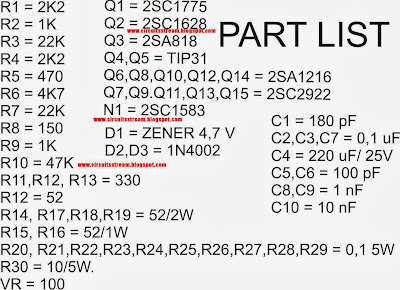
Parts List

Build a 1000W Power Amplifier Circuit Schematic Diagram with Explanation
Circuit uses power transistors pair of 5 x 5 x 2SA1216 and 2SC2922 and 2SC1583 use a differential amplifier that actually contains 2 pieces of transistors that are in containers together. Why use such built-in amplifier differental tujuanya so identical / similar, could have uses 2 separate transistors but can result in amplifier so it is not symmetrical.

Tips combining speaker


Build a 1000W Power Amplifier Circuit Schematic Diagram with Explanation
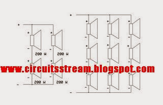
To get the speakers with great power combining techniques can be used in parallel series, combining each group of speakers should sepaker they will have the same impedance, the same type (Woofer, Mid Range or tweeter) and the same power. Number of merging these speakers should consists of 4 , 9, 16 ff, see picture

Example
The number of speakers have 4 pieces each of its 200 Watt power generated will be a speaker at = 200 x 4 = 800 Watt. If there are 9 speakers 200 W then the result = 9 x 200 W = 1800 Watt.

3000 watt power inverter 12V DC to 230V AC With Circuit schematic & Explanation

Tags

3000 watt power inverter 12V DC to 230V AC


3000 watt power inverter 12V DC to 230V AC With Circuit schematic & Explanation
Circuit Diagram of 3000 watt power inverter 12V DC to 230V AC

 Sine-wave voltage and conventional square wave voltage with both 230 Volt rms 3000 watt power inverter 12V DC to 230V AC With Circuit schematic & Explanation
Fig. 2: Sine-wave voltage and conventional square wave voltage with both 230 Volt rms

 Square wave voltage with duty cycle 25% for 230 Volt rms ("modified sine")
Fig. 3: Square wave voltage with duty cycle 25% for 230 Volt rms ("modified sine")


PCB Layout:3000 watt power inverter 12V DC to 230V AC

3000 watt power inverter 12V DC to 230V AC With Circuit schematic & Explanation


Component Placement: 3000 watt power inverter 12V DC to 230V AC


3000 watt power inverter 12V DC to 230V AC With Circuit schematic & Explanation


output voltage with no load or inductive load. 3000 watt power inverter 12V DC to 230V AC With Circuit schematic & Explanation
fig.: output voltage with no load or inductive load.


resistor 0,001 Ohm made of high-grade steel sheet metal  3000 watt power inverter 12V DC to 230V AC With Circuit schematic & Explanation
fig.: resistor 0,001 Ohm made of high-grade steel sheet metal

Control electronics | 3000 watt power inverter 12V DC to 230V AC


fig.: control electronics on strip hole plate (previous version) and PCB of the "professional edition"


Assembly of the mosfet-transistors on the heat sink | 3000 watt power inverter 12V DC to 230V AC


heat sink, mosfet transistors, connections.
fig.: heat sink, mosfet transistors, connections.


Final assembly | 3000 watt power inverter 12V DC to 230V AC


1500 VA inverter with 2 parallel transformers and 1000 VA inverter
fig.: 1500 VA inverter with 2 parallel transformers and 1000 VA inverter


Source:http://www.qsl.net

Simple Light Audio Transmitter Circuit Schematic Diagram with explanation

This is the Simple Light Audio Transmitter Circuit Diagram. In the visible-light transmitter, a 7805 voltage regulator is connected in a variable-voltage configuration, and an audio signal is fed to the common input, to modulate the output voltage. The modulated output voltage is used to transmit intelligence via an incandescent lamp.
Simple Light Audio Transmitter Circuit Schematic Diagram with explanation


Simple Light Audio Transmitter Circuit Schematic Diagram with explanation

Op-Amp Dc Offset Shift Circuit Schematic with Explanation


This is the simple Op-Amp Dc Offset Shift Circuit Diagram. The dc values of op-amp offsets can`t always be taken for granted when delivering ac outputs. No device is ever exactly symmetrical for maximum positive slew rate versus maximum negative slew rate. Consequently, there is always some range of output slew rates in which the device used limits in one direction more severely than in the other.


Op-Amp Dc Offset Shift Circuit Diagram


Op-Amp Dc Offset Shift Circuit Schematic with Explanation


What results in rectification of the ac signal and an apparent shift of the dc offset. This test circuit can check for the shift phenomenon. The accompanying table and graph illustrate the results obtained for four devices, all of different types.As frequency and slew rate are increased, the effect can be either relatively abrupt (LF412CN and NE55532N) or relatively gradual (LF358J and TL0820P).

Cimple LED Flasher Circuit Schematic With Explation


Cimple LED Flasher Circuit Schematic With ExplationThis is a simple circuit diagram .Here we have used common IC LM317 T.You can choose flowing current according to the chart this circuit can be operated with 9V to 20V.


Cimple LED Flasher Circuit Schematic With Explation


Note

# Build this circuit on a PCB

Advertisement