Showing posts with label Power Amplifier. Show all posts

IC-7905 Stereo Power Amplifier Circuit Project with schematic

79xx is a widely known series of low-cost, fixed-negative-voltage regulators. These integrated circuits are available with output current of 100-150 mA (L series), 0.4-0.5A (M series), up to 1A (standard series), etc. They can be used in many applications other than regulators, audio power amplifier being one of them.  As shown in the circuit diagram, a simple stereo audio amplifier is built around two 7905 negative-voltage regulators (IC1 and IC2) and a few discrete components. The 7905 IC (a -5V regulator) used here is readily available. However, the circuit will also work with other 79XX regulators if appropriate power supply is used. Both channels shown in the diagram are identical. Hence the description below is only for the first channel. The quality of the output signal is within acceptable limits.

Stereo Power Amplifier Circuit Diagram:

 IC-7905 Stereo Power Amplifier Circuit Project with schematic

Regulator IC 7905 works as an amplifier for the voltages applied to common pin2 (Ground or GND). The minimal voltage drop over the standard 7905 is around 2V and it depends on the output current. Feedback resistors in the IC set the gain of the channel internally. The amplifier is a class-A audio amplifier. The regulator IC produces the negative output signal.

Resistor R3 provides the positive signal. It limits the maximum output current of the regulator during the negative half period of the amplified sinusoidal signal. The minimal applicable value of R3 for the regulator 7905 is 8.2 to 10 ohms per 5W.  Optimisation of the value of R3 depends on the output voltage of the regulator, negative power supply (–5V) and load resistance of loudspeaker (LS1). If the required output current for LS1 is below 100 mA, the value of resistor R3 can be 33 to 51 ohms per watt.

Normally, the load resistance of the loudspeaker should be higher than of R3 in order to obtain a large peak-to-peak amplitude. But this can be neglected in order to obtain lower power dissipation on R3 and the IC. The circuit works with any load resistance (R3 in parallel with LS1 as the load) under the condition that the regulator is not overloaded with current and power dissipation. However, it is preferable to use a loudspeaker with a high resistance (8 ohms, 16 ohms or more). The amplifier works well with low-impedance headphones having a resistance of 24 to 32 ohms. The voltage difference between the ground pin of 7905 and the output pin is fixed internally.

The input resistance of the amplifier is relatively low and depends on potentiometer VR1 and input resistance of the ground pin. Practically, any stereo output capable of driving 24- or 32-ohm headphones and loudspeakers can drive the input of the stereo amplifier with 7905. If VR1 is removed, the amplifier will still work but there will be more distortion. Therefore potentiometer VR1 is used to provide sufficient variable audio signal.  The values of output capacitors C10 and C11 are usually between 0.1 µF and 1 µF. A small resistance can be connected in series with them if needed. S2 is the on/off switch. Switch S1 is for mono/stereo selection. When switch S1 is closed, the amplifier works as a two-way mono amplifier. If S1 is open, the amplifier works as a stereo amplifier.

The circuit is powered by a 12V battery. The positive terminal of the battery is the common node. The negative terminal is connected to pin 2 of IC1, which is the –12V supply line. The maximum operating voltage can be up to –35V. If no input signal is applied, the DC voltage on the output of the regulator 7905 should be around –5V, which depends to some extent on the value of VR1. The maximum output current of 7905 can be up to 1A and the maximum power dissipation is up to 15W. IC 7905 has internal thermal protection.

Assemble the circuit on a general-purpose PCB and enclose in a suitable cabinet. Fix the stereo female jack on the front panel and speaker to the rear side of the cabinet, and the 12V battery inside the cabinet. Fix LED1 and switches S1 and S2 too on the front panel of the cabinet. Mount the regulator IC 7905 on a heat-sink with thermal resistance below 15°C/W. The metallic part on the case is internally connected with the input pin of the regulator.

Author : Petre tzv. Petrov - Copyright : EFY

Stereo Power Amplifier Using IC 7905

For a few pounds you can buy a kit from any automotive accessory shop that will allow your car to be fitted with a central-locking door system. Such a kit essentially comprises a number of motors. There is also a control unit that enables the whole system to function. Here we show an example of such a unit. There are 5-wire motors and 2-wire motors. The 5-wire version is used in doors that have a key-lock.

Car Central Locking System Project Image: 

Car Central Locking System Project


There are 2 connections for the motor itself and 3 connections for the sensor part (an ‘open’ and a ‘close’ contact). These sensors determine whether the door is to be unlocked or locked. If there is no key lock in the door, these sensors are superfluous and a 2-wire motor can be used.

The polarity of the motor determines whether the locking mechanism goes up or down. By making a circuit that simply reverses the polarity of the motor, the door can be either locked or unlocked. The winding of the motor is connected between M1 and M2 in the schematic. When relay Re1 is energised, all motors will, for example, rotate anti-clockwise. By activating Re2 the motors will rotate clockwise. This depends on the actual polarity of the motor, of course.

The sensors are connected to R1 and R10. Here you have to pay careful attention. If Re1 causes the door to unlock, then Re1 has must obviously be connected to the ‘open’ contact. In that case, Re2 is for locking the doors and R10 is then connected to the ‘close’ contact. The R/C-combinations R16/C3 and R15/C4 ensure that the relays are energised for a certain amount of time (obviously this can be changed if this time is too short or too long for your doors).

Car Central Locking System Circuit Diagram:


System Circuit Diagram

This time has to be just long enough to lock or unlock the doors. The third wire of the sensors is the common and has to be connected to +12 V. The RC circuits at the inputs Sopen en Sclose ensure that the motors are driven only once when the door is locked or unlocked.  In addition, there is a provision to allow the unit to be connected to a car alarm. There are two types of alarm available, with positive or negative control. In order to make the unit universally applicable, both types of alarm can be used. The circuit around T3 and T4 makes this possible. The diode inputs (D3 and D8) react to a rising edge, R6 and R8 react to a falling edge. An RC time constant is used here as well to ensure that both relays are energised only once.

Maybe this is stating the obvious: a motor unit has to be built into each door. All motor wires and sensor wires are connected in parallel to the electronics. The actual type of relay is not critical. The type indicated has the following proper-ties: coil 12 V/400 Ω; max. switching current 12 A (AC), max. switching power 1200 VA.

PCB Layout:

PCB Layout


Finally, a car is a hostile environment for electronics. Ensure good connections, use automotive connectors and crimp these on the wires using the appropriate crimping tool. Solder connections in wires are best avoided. They have the tendency to break where the wire transitions into the solder connection when the wire is subject to vibration. Fasten the wires at regu-lar intervals.

scheme power amplifier 20W RADIO circuit schemati with explanation

scheme power amplifier 20W RADIO

scheme 20W power amplifier (AUTO BOOSTER FOR CAR-MOTORCYCLE 20 WATTS)

scheme power amplifier 20W RADIO circuit schemati with explanation


The assembly described offers a boost of 20 watts that will allow you to realize a power amplifier with which one can increase the output power of a car radio up to 20 Watts maximum.

scheme power amplifier 20W RADIO circuit schemati with explanation


The input IN is connected to the output of the car radio, output U is connected to the speaker as Represents the scheme.
It is very important to ensure that the speaker has no connection to the chassis ( mass) ; otherwise, integrated circuit IC1, a TDA 2004 would be instantly destroyed.For mounting of components, carefully monitor implementation of the scheme composanls. The alimenlalion will continue at 12 Volts.


LIST OF ELECTRONIC COMPONENTS: All resistors are of 1/4 watt unless statedotherwise. R = 100 Ohms R2 = l, 5Kohms R3 = 180 Ohm R4 = 470 Ohms R5 = 10hmR6 = 10hm Cl = 0, lpFpol. C2 = 1000pFceramique . C3-10uF16Velec. C4 = 0, luFpol.C5 = 0,22uFpol. C6 = 0,22yFpol. C7-0,22uFpol. IC1 = TDA2004 1 Heatsink


Build a 300 Watt Subwoofer Power Amplifier Circuit Diagram


The output devices are MJL4281A (NPN) and MJL4302A (PNP), and feature high bandwidth, excellent SOA (safe operating area), high linearity and high gain. Driver transistors are MJE15034 (NPN) and MJE15035 (PNP). All devices are rated at 350V, with the power transistors having a 230W dissipation and the drivers are 50W.

Having built a P68 using these transistors, I recommend them highly - the amplifier is most certainly at its very best with the high gain and linearity afforded by these devices. Note that there are a few minor changes to the circuit (shown below).

High power amps are not too common as projects, since they are by their nature normally difficult to build, and are expensive. A small error during assembly means that you start again - this can get very costly. I recommend that you use the PCB for this amplifier, as it will save you much grief. This is not an amp for beginners working with Veroboard!

The amplifier can be assembled by a reasonably experienced hobbyist in about three hours. The metalwork will take somewhat longer, and this is especially true for the high continuous power variant. Even so, it is simple to build, compact, relatively inexpensive, and provides a level of performance that will satisfy most requirements.

300W Sub woofer Power Amplifier Circuit Diagram

Build a 300 Watt Subwoofer Power Amplifier Circuit Diagram

Fig 1
WARNINGS:
  • This amplifier is not trivial, despite its small size and apparent simplicity. The total DC is over 110V, and can kill you.
  • The power dissipated is such that great care is needed with transistor mounting.
  • The S300 is intended for intermittent duty on 4 Ohm loads, as will normally be found in a subwoofer. It is NOT intended for PA or any other continuous duty, and although it may work fine for may years, I absolutely do not recommend this.
  • For continuous duty, do not use less than 8 Ohms.
  • There is NO SHORT CIRCUIT PROTECTION. The amp is designed to be used within a subwoofer enclosure, so this has not been included. A short on the output will almost certainly destroy the amplifier.
DO NOT ATTEMPT THIS AMPLIFIER AS YOUR FIRST PROJECT

Please note that this amp is NOT designed for continuous high power into 4 Ohms. It is designed for intermittent duty, suitable for an equalized sub woofer system (for example using the ELF principle - see the Project Page for the info on this circuit). Where continuous high power is required, another 4 output transistors are needed, wired in the same way as Q9, Q10, Q11 and Q12, and using 0.1 ohm emitter resistors.

Continuous power into 8 ohms is typically over 150W, and it can be used in the form shown at full power into an 8 ohm load all day, every day. The additional transistors are only needed if you want to do the same thing into 4 ohms!

The circuit is shown in Figure 1, and it is a reasonably conventional design. Connections are provided for the Internal SIM (published elsewhere on the Project Pages), and filtering is provided for RF protection (R1, C2). The input is via a 4.7uF bipolar cap, as this provides lots of capacitance in a small size. Because of the impedance, little or no degradation of sound will be apparent. A polyester cap may be used if you prefer - 1uF with the nominal 22k input impedance will give a -3dB frequency of 7.2Hz, which is quite low enough for any sub.
The input stage is a conventional long-tailed pair, and uses a current sink (Q1) in the emitter circuit. I elected to use a current sink here to ensure that the amp would stabilise quickly upon application (and removal) of power, to eliminate the dreaded turn on "thump". The amp is actually at reasonably stable operating conditions with as little as +/-5 volts! Note also that there are connections for the SIM (Sound Impairment Monitor), which will indicate clipping better than any conventional clipping indicator circuit. See the Project Pages for details on making a SIM circuit.
The Class-A driver is again conventional, and uses a Miller stabilisation cap. This component should be either a 500V ceramic or a polystyrene device for best linearity. The collector load uses the bootstrap principle rather than an active current sink, as this is cheaper and very reliable (besides, I like the bootstrap principle :-)

All three driver transistors must be on a heatsink, and D2 and D3 should be in good thermal contact with the driver heatsink. Neglect to do this and the result will be thermal runaway, and the amp will fail.

C11 does not exist on this schematic, so don't bother looking for it. It was "mislaid" when the schematic was prepared, and I didn't notice until someone asked me where and what it was supposed to be. Sorry about that.
It is in the output stage that the power capability of this amp is revealed. The main output is similar to many of my other designs, but with a higher value than normal for the "emitter" resistors (R16, R17). The voltage across these resistors is then used to provide base current for the main output devices, which operate in full Class-B. In some respects, this is a "poor-man's" version of the famous Quad "current dumping" circuit, but without the refinements.

Although I have shown MJL4281A and MJL4302A output transistors, because they are new most constructors will find that these are not as easy to get as they should be. The alternatives are MJL21193/ MJL21194
Build a 300 Watt Subwoofer Power Amplifier Circuit Diagram
Fig 2

Note: It is no longer possible to recommend any Toshiba transistors, since they are the most commonly counterfeited of all. The 2SA1302 and 2SC3281 are now obsolete - if you do find them, they are almost certainly fakes, since Toshiba has not made these devices since around 1999~2000.

Use a standard green LED. Do not use high brightness or other colors, as they may have a slightly different forward voltage, and this will change the current sink's operation - this may be a miniature type if desired. The resistors are all 1/4W (preferably metal film), except for R10, R11 and R22, which are 1W carbon film types. All low value resistors (1 ohm and 0.1 ohm) are 5W wire wound types.

Because this amp operates in "pure" Class-B (something of a contradiction of terms, I think), the high frequency distortion will be relatively high, and is unsuited to high power hi-fi. At the low frequency end of the spectrum, there is lots of negative feedback, and distortion is actually rather good, at about 0.04% up to 1kHz.

Power output into 4 ohms is over 250W continuous, and for transients exceeds 300W easily. Use of a big power transformer and massive filter caps will allow the amp to deliver close to 350W continuous, but if you really want to use it like that, I very strongly recommend the additional output transistors (see above comments on this topic).

Power Dissipation Considerations
I have made a lot of noise about not using this amp for continuous duty into 4 ohms without the extra transistors. A quick calculation reveals that at the worst case, the output and transistor voltage will be the same - i.e. at 28V. With 28V, load (and transistor) current is 7A, so the instantaneous dissipation is therefore 28 * 7 = 196W. This means that the four final transistors do most of the work, with the others having a relatively restful time.

Since I like to be conservative, I will assume that they contribute no more than about 1.5A (which is about right). This means that they only dissipate 48W, with the main O/P devices dissipating a peak of 74W each. The specified transistors are 130W, and the alternatives are 150W, so where is the problem?

The problem is simple - the rated dissipation for a transistor is with a case temperature of 25°C. As the amp is used, each internal transistor die gets hot, as does the transistor case - the standard derating curves must be applied. Add to this the reactive component as the loudspeaker drives current back into the amp, and it becomes all too easy to exceed the device dissipation limits.

Figure 1A shows the doubled output stage, with Q9, Q10, Q11 and Q12 simply repeated - along with the emitter resistors. Each 1/2 stage has its own zobel network and bypass caps as shown, as this is the arrangement if the dual PCB version is built. When you have this many power transistors, the amp will happily drive a 4 ohm load all day - with a big enough heatsink, and / or forced cooling (highly recommended, by the way).

A Few Specs and Measurements

The following figures are all relative to an output power of 225W into 4 ohms, or 30V RMS at 1kHz, unless otherwise stated. Noise and distortion figures are unweighted, and are measured at full bandwidth. Measurements were taken using a 300VA transformer, with 6,800uF filter caps. Mains voltage was about 4% low when I did the tests, so power output will normally be slightly higher than shown here if the mains are at the correct nominal voltage.

Gain27dB
Power (Continuous)240W (4 ohms)

153W (8 ohms)
Peak Power - 5 ms185W (8 ohms)
Peak Power - 10 ms172W (8 ohms)
Input Voltage1.3V RMS
Noise-63dBV (ref. 1V)
S/N Ratio92dB
Distortion0.4%
Distortion (@ 4W)0.04% (1 Khz)
Distortion (@ 4W)0.07% (10 kHz)
Slew Rate> 3V/us
Power Bandwidth30 kHz
These figures are quite respectable, especially considering the design intent for this amp. While it would not be really suitable for normal hi-fi, even there it is doubtful that any deficiencies would be readily apparent, except perhaps at frequencies above 10kHz. While the amp is certainly fast enough (and yes, 3V/us actually is fast enough - full power is available up to 30kHz), the distortion will be a bit too high.

Note that the "peak power" ratings represent the maximum power before the filter caps discharge and the supply voltage collapses. I measured these at 5 milliseconds and 10 milliseconds. Performance into 4 ohm loads will not be quite as good, as the caps will discharge faster. The supply voltage with zero power measured exactly 56V, and collapsed to 50.7V at full power into 8 ohms, and 47.5V at full power into 4 ohms.

Photo of amp
Photo of Completed Prototype

The photo does not show the silk screened component overlay, since this is the prototype board. The final boards have the overlay (as do all my other boards).

As can be seen, this is the single board version. The driver transistors are in a row, so that a single sheet aluminium heatsink can be used for all three. Holes are provided on the board so the driver heatsink can be mounted firmly, to prevent the transistor leads breaking due to vibration. This is especially important if the amp is used for a powered subwoofer, but will probably not be needed for a chassis mounted system.
The driver and main heatsinks shown are adequate for up to 200W into 4 ohms with normal program material. The power transistors are all mounted underneath the board, and the mounting screw heads can be seen on the top of the board.

Deceptively simple, isn't it?

Power Supply

WARNING: Mains wiring must be performed by a qualified electrician - Do not attempt the power supply unless suitably qualified. Faulty or incorrect mains wiring may result in death or serious injury.
The basic power supply is shown in Figure 2. It is completely conventional in all respects. Use a 40-0-40 V transformer, rated at 300VA for normal use. For maximum continuous power, a 500VA or bigger transformer will be needed. This will give a continuous power of about 350W, and peak power of close to 400W is possible with a good transformer. Remember my warnings about using the amp in this way, and the need for the additional output transistors.

Build a 300 Watt Subwoofer Power Amplifier Circuit Diagram
Figure 2 - Basic Power Supply Circuit
For 115V countries, the fuse should be 6A, and in all cases a slow blow fuse is required because of the inrush current of the transformer.

C1 must be rated for 240V AC (or 120V AC) operation - do not use standard 250V DC caps under any circumstance, as they will fail, and R1 will explode! This is not intended as humour - this is fact! C1 and R1 may be omitted in most cases, and if you cannot get a mains rated capacitor I suggest that you don't install these components.

The supply voltage can be expected to be higher than that quoted at no load, and less at full load. This is entirely normal, and is due to the regulation of the transformer. In some cases, it will not be possible to obtain the rated power if the transformer is not adequately rated.

Bridge rectifiers should be 35A types, and filter capacitors must be rated at a minimum of 63V. Wiring needs to be heavy gauge, and the DC must be taken from the capacitors - not from the bridge rectifier.

Although shown with 4,700uF filter capacitors, larger ones may be used. Anything beyond 10,000uF is too expensive, and will not improve performance to any worthwhile degree. Probably the best is to use two 4,700uF caps per side (four in all). This will actually work better than a single 10,000uF device, and will be cheaper as well.

NOTE: It is essential that fuses are used for the power supply. While they will not stop the amp from failing (no fuse ever does), they will prevent catastrophic damage that would result from not protecting the circuit from over-current conditions. Fuses can be mounted in fuseholders or can be inline types. The latter are preferred, as the supply leads can be kept as short as possible. Access from outside the chassis is not needed - if the fuses blow, the amplifier is almost certainly damaged.

Build a 1000W Power Amplifier Circuit Schematic Diagram with Explanation

I think you've seen or even have an active speaker and there is written 1500 watts PMPO (Peak Music Power Output), make no mistake this is different from Power Amplifier Active Speaker, I often dismantle such Active Speaker in it only a power with power no more than 150 watts by using the transformer 2-3 Ampere. PMPO is not a real power which is issued by the Power Amplifier, but counting all the speakers that there is, for example: if there are 5 pieces of speakers on each channel and each speaker has a power of 10 W then it is 100 W PMPO.

1000W Power Amplifier Circuit Diagram


Build a 1000W Power Amplifier Circuit Schematic Diagram with Explanation
While this 1000 Watt Power Amplifier minimal use transformer 20 Ampere. And the output of Power Amplifier DC voltage contains approximately 63 volts, with currents and voltages of this magnitude, this 1000 Watt Power Amplifier will not hesitate hesitate to destroy your woofer speakers to connect. To overcome that then before the speaker on connects to 1000 Watt Power Amplifier must be in pairs Speaker Protector.

Actually if you want to create a Power Amplifier with great power does not have to make a Power Amplifier with great power. Example: you want to create a Power Amplifier with 10 000 Watt power. You do not have to assemble a Power Amplifier with power of 10,000 watts, but you assemble the power Power Amplifier Small but many, such as you assemble the Power Amplifier with 1000 Watts of power for as many as 10 pieces, it will produce 10 000 Watt Power Amplifier helpless.

Parts List

Build a 1000W Power Amplifier Circuit Schematic Diagram with Explanation
Circuit uses power transistors pair of 5 x 5 x 2SA1216 and 2SC2922 and 2SC1583 use a differential amplifier that actually contains 2 pieces of transistors that are in containers together. Why use such built-in amplifier differental tujuanya so identical / similar, could have uses 2 separate transistors but can result in amplifier so it is not symmetrical.

Tips combining speaker


Build a 1000W Power Amplifier Circuit Schematic Diagram with Explanation
To get the speakers with great power combining techniques can be used in parallel series, combining each group of speakers should sepaker they will have the same impedance, the same type (Woofer, Mid Range or tweeter) and the same power. Number of merging these speakers should consists of 4 , 9, 16 ff, see picture

Example
The number of speakers have 4 pieces each of its 200 Watt power generated will be a speaker at = 200 x 4 = 800 Watt. If there are 9 speakers 200 W then the result = 9 x 200 W = 1800 Watt.

GUITAR OR HI-FI Power Amplifiers 12Watt tube 6BM8 + 6KG6 (EL509) Circuit Schematic With Explanation

GUITAR OR HI-FI Power Amplifiers 12Watt tube 6BM8 + 6KG6 (EL509) Circuit Schematic With Explanation


HI FI audio power amplifieers with tone{2x12 watt}


The TDA2616 is a hi-fi stereo amplifier designed for mains fed applications, such as stereo radio and TV. The circuit is optimally designed for symmetrical power supplies, but is also well-suited to asymmetrical power supply systems.
An output power of 2 ´ 12 W (THD = 0.5%) can be delivered into an 8 Wload with a symmetrical power supply of ±16 V. The gain is internally fixed at 30 dB, thus offering a low gain spread and a very good gain balance between the two amplifiers (0.2 dB).
A special feature is the input mute circuit. This circuit disconnects the non-inverting inputs when the supply voltage drops below ±6V, while the amplifier still retains its DC operating adjustment. The circuit features suppression of unwanted signals at the inputs, during switch-on and switch-off.
The mute circuit can also be activated via pin 2. When a current of 300 mA is present at pin 2, the circuit is in the mute condition. The device is provided with two thermal protection circuits.
One circuit measures the average temperature of the crystal and the other measures the momentary temperature of the power transistors. These control circuits attack at temperatures in excess of +150 °C, so a crystal operating temperature of max. +150 °C can be used without extra distortion.


FEATURES
· Requires very few external components
· No switch-on/switch-off clicks
· Input mute during switch-on and switch-off
· Low offset voltage between output and ground
· Excellent gain balance of both amplifiers
· Hi-fi in accordance with IEC 268 and DIN 45500
· Short-circuit proof and thermal protected
· Mute possibility.
S:elec-circuits.blogspot.com

LM1875 50 watt Hi Fi power amplifier

The LM1875 is a monolithic power amplifier offering very low distortion and high quality performance for consumer audio applications.
The LM1875 delivers 20 watts into a 4Ω or 8Ω load on ±25V supplies. Using an 8Ω load and ±30V supplies, over 30 watts of power may be delivered. The amplifier is designed to operate with a minimum of external components. Device overload protection consists of both internal current limit and thermal shutdown.
The LM1875 design takes advantage of advanced circuit techniques and processing to achieve extremely low distortion levels even at high output power levels. Other outstanding features include high gain, fast slew rate and a wide power bandwidth, large output voltage swing, high current capability, and a very wide supply range. The amplifier is internally compensated and stable for gains of 10 or greater.

This circuit diagram 50Watt Hi-Fi Power Amplifier based on LM1875 ICs and 2SA1943 – 2SC5200 bridge transistors. It has good input sensitivity, low distortion, good operating stability and full protection against overloads and output short-circuits. It can be used as a booster amplifier for existing small systems or to drive a second pair of speakers besides the ones already connected to the system. The board needs a symmetrical power supply of ±18V – 25V dc/4A and can be connected to 8 or 4 Ohm speakers. Large heat sink is required for this circuit. Diagram shown below indicates only the left channel. Make two circuits for for stereo version.
The output coil L1 using φlmm enameled wire wound resistor in R10 3W without being tightly wound 10 turns on. Power section using dual-18V 150W high-quality toroidal transformer, 35V/4700μF the filter capacitor 4, 35V/100μF two, 100V/0.1μF two, insurance management FUSE1, FUSE2 use 4A.

Technical Specifications:
  • Supply voltage = ±25Vdc/4A symmetrical (see text)
  • Current consumption = 3A maximum
  • Input impedance = 47K Ohms
  • Input sensitivity = 650 mV
  • Signal to noise ratio = 90 dB
  • Frequency response = 20 - 20,000 Hz ± 1 dB
  • Distortion = 0.5 % maximum
  • Load impedance = 4 - 8 ohm
Parts:
R1 = 470R – 1/2w
R2 = 47k – 1/2w
R3 = 1,2K – 1/2w
R4 = 1R – 1,4R - 4w
R5 = 1R – 1,4R - 4w
R6 = 0.22R - 4w
R7 = 0.22R - 4w
R8 = 47k – 1/2w
R9=22R – 3w
R10=10R – 3w


C1 = 4,7uf-25V
C2 = 100uF-25V
C3 = 1000uF -62V
C4 = 1000uF -62V
C5 = 100nF-62V
C6 = 100nF-62V

L1 = (see text)

Q1 = 2SC5200
Q2 = 2SA1943

IC = LM1875
S:elec-circuits.blogspot.com

a tiny aluminium box and Nanoo chip amplifier

Here is another one of Mark's projects which has been added to DIY Audio Projects website. His latest creation is the compact DIY Nanoo Chip Amplifier (LM3875 Gainclone).

Nanoo Chip Amplifier (LM3875 Gainclone)
The enclosure for the amplifier is a tiny aluminum box that measures 119 X 94 X 34 mm. The amplifier is based around the popular LM3875 chip using point-to-point wiring. Power to the amplifier is provided via an external power supply which is also housed in an aluminum enclosure.

IRF9540 - IRF540 based 100 W 8 ohms MOSFET amplifier

The Schematic Diagram is a basic MOSFET amplifier. Output power is 100 Wrms under 8 ohms or 160 Wrms under 4 ohms with distortion is 0.001 %. Bandwidth at -3 db is from 4 Hz to 100 Khz .
Input sensitivity is 1.2 volts. The gain of 27DB is archived by R7/R6. It may be modified by changing R7 value. Transistors T5 and T6 makes the second differential stage. Transistors T3 and T4 works as a current mirror source. They push the second differential stage to drain equal current. Doing so we get a high gain and an excellent linearity. Output MOSFET transistors works in AB class, their quiescent current is set at 100 mA trough P1. For setting quiescient current, you must set P1 in minimal resistance, place a multimeter in mV DC range on R14 or R15 leads, turn slowly the screw until you read a 33 mV value, which correspond to a 100 mA quiescent current.
F1 and F2 works as an elementary output short-circuit protection. The power supply must have a value between 45 and 55 Volts DC (positive and negative). One heatsink with a thermal resistance less of 2° C / W is required.
All resistors are 1% metal film 1/4 watt. Before connecting a speaker to the amplifier output, connect a multimeter to the output and look on DC output voltage. This level must not be greater than 50 mV. If it is so, check all amplifier for error. Also, change T2 with another device and check again. This amplifier is very simple to build and low cost.
Part List
C1 = 2,2 µF-100 V
C2 = 330 pF-100 V
C3 = 100 nF -100 V
C4 = 100 µF 63 V
C5, C6 = 18 pF
C7 = 100 nF
R1, R3 = 47 K
R2 = 2K2
R4, R5 = 3K9
R6 = 1 K
R7 = 27 K
R8, R9, R11 = 100 ohms
R10 = 10 K
R12, R13 = 470 ohms
R14, R15 = 0.33 ohms 5 watts
R16 = 10 ohms 3 watts
T1, T2 = 2N5401, ZTX558, BC556B
T3, T4 = BF470, MJE350, 2SB649
T5, T6 = BF469, MJE340, 2SD669
T7 = IRF540, IRFP240, 2SK1530, 2SJ162, BUZ900DP, BUZ901DP
T8 = IRF9540, IRFP9240, 2SJ201, 2SK1058, BUZ905DP,
P1 = 2K5 trimmer
F1, F2 = 3 A

power supply
One 2x40 volts 225 VA transformer is exactly what we need for one mono amplifier. For a stereo amplifier, one 2x40 volts 500 VA transformer is required.
Use at least 4x6800 µF 63-80 V reservoir capacitors. The more caps you use, the better the ripple rejection.
4K7 5W resistors are used to discharge reservoir capacitors once mains is set off.


LM4702 Driver Chip based MOSFET Power Amplifier(120w)


National Semiconductor has been fast at work designing analog products for the high-end audiophile market. As for­tune would have it, these products such as the LM4780 Power Amplifier Chip and the LM4702 Driver Chip are easy to implement into high-quality designs for the audio DIYer.
National recently introduced the LM4702, a high-voltage driver chip that interfaces bipolar or MOSFET output devices. The LM4702 provides two small signal, input stages and voltage amplifica­tion stages (VAS). All you need to do is design a suitable bias system and output stage.
Not to be outdone in making the job easy for us amateurs, National provides a comprehensive design outline, guide to printed circuit board construction, ideas for the power supply, bill of materials, and suggested layout. In an application note dated May 20061, the company de­scribed an amplifier using high-qual­ity construction techniques and off-the-shelf passive components. The result is an amplifier with a vanishingly low level of distortion, 0.0006%.

1500w power amplifier-40hms

This project is mainly in answer to those for whom no amount of power is enough. I have lost count of the number of times people have asked if it's alright to increase the supply voltage on every circuit published, and in general the answer is no - it's not alright. Every design on this site is optimised for the stated power. There is always some flexibility, but you must be very careful to make sure that transistor safe operating area (SOA) is not exceeded. There is also a maximum voltage for any semiconductor, and devices must be selected to ensure they are used within their ratings

ic TDA2050 based 32W HI-FI AUDIO POWER AMPLIFIER


The TDA 2050 is a monolithic integrated circuit in Pentawatt package, intended for use as an audio class AB audio amplifier. Thanks to its high power capability the TDA2050 is able to provide up to 35W true rms power into 4 ohm load @ THD = 10%, VS = ±18V, f = 1KHz and up to 32W into 8ohm load@ THD = 10%, VS = ±22V, f = 1KHz.
Moreover, the TDA 2050 delivers typically 50W music power into 4 ohm load over 1 sec at VS= 22.5V, f = 1KHz.
The high power and very low harmonic and crossover distortion (THD = 0.05% typ, @ VS = ±22V, PO = 0.1 to 15W, RL=8ohm, f = 100Hz to 15KHz) make the device most suitable for both HiFi and high class TV sets
  • HIGH OUTPUT POWER
  • (50W MUSIC POWER IEC 268.3 RULES)
  • HIGH OPERATING SUPPLY VOLTAGE (50V)
  • SINGLE OR SPLIT SUPPLY OPERATIONS
  • VERY LOW DISTORTION
  • SHORT CIRCUIT PROTECTION (OUT TO GND)
  • THERMAL SHUTDOWN
PARTS LIST
R1----22K
R2----680
R3----22K
R4----2.2

C1----1mf
C2----22mf
C3----100nf
C4----100nf
C5----220mf
C6----220mf
C7----0.47mf
IC----TDA2050

integrated output amplifier used in motor vehicles and other battery operated applications


The integrated output amplifier described in this article consists of little more than one integrated circuit. It is intended especially for use in motor vehicles and other battery operated applications. Although it appears simple and hardly worth looking at, the amplifier can produce an appreciable audio power output.

technical data Properties High power output through Class-H operation
Low power dissipation during reproduction of music signals
Proof against short-circuits
Protection against excessive temperatures
Standby switch
No power-on or power-off clicks
Visible error indication
Measurement results (at Ub=14.4 V)
Supply voltage 8–18 V
Sensitivity 760 mV r.m.s.
Input impedance 70 kΩ
Power output 54 W r.m.s. into 4 Ω (f=1 kHz; THD+N=1%)
Harmonic distortion (THD+N) at 1 W into 4 Ω: 0.046% (1 kHz)
0.29% (20 kHz)
at 35 W into 4 Ω: 0.12% (1 kHz)
0.7% (20 kHz)
Signal-to-noise ratio (with 1 W into 4 Ω) 88 dBA
Power bandwidth 7.5 Hz – 185 kHz (at 25 W into 4 Ω)
Quiescent current about 135 mA (‘on’)

COMPONENTS LIST
Resistors:
R1 = 1MΩ
R2 = 4kΩ7
R3 = 1kΩ
R4 = 100kΩ
Capacitors:C1,C2 = 470nF
C3,C4 = 10μF 63V radial
C5,C6,C8 = 4700μF 25V radial
(18mm max. dia., raster 7.5 mm)
C7 = 100nF, raster 5 mm
Semiconductors:
D1 = high-efficiency-LED
IC1 = TDA1562Q (Philips)
Miscellaneous:
S1 = single-pole on/off switch
Four spade connectors, PCB mount
Heatsink for IC1 (Rth<2.5>

300W Power Amplifier For Subwoofer

The 300W Amplifier circuit is shown it is a reasonably conventional design. Connections are provided for the Internal SIM, and filtering is provided for RF protection (R1, C2). The input is via a 4.7uF bipolar cap, as this provides lots of capacitance in a small size. Because of the impedance, little or no degradation of sound will be apparent. A polyester cap may be used if you prefer - 1uF with the nominal 22k input impedance will give a -3dB frequency of 7.2Hz, which is quite low enough for any sub.
Rangkaian 300W Power Amplifier For Subwoofer
Continuous power into 8 ohms is typically over 150W (250W for ±70V supplies), and it can be used without additional transistors at full power into an 8 ohm load all day, every day. The additional transistors are only needed if you want to do the same thing into 4 ohms at maximum supply voltage

Although I have shown MJL4281A and MJL4302A output transistors, because they are new most constructors will find that these are not as easy to get as they should be. The alternatives are MJL3281/ MJL1302 or MJL21193/ MJL21194.

Because this amplifier circuit operates in "pure" Class-B (something of a contradiction of terms, I think), the high frequency distortion will be relatively high, and is probably unsuited to high power hi-fi. At the low frequency end of the spectrum, there is lots of negative feedback, and distortion is actually rather good, at about 0.04% up to 1kHz. My initial tests and reports from others indicate that there are no audible artefacts at high frequencies, but the recommendation remains.

Circuit from: www.sound.westhost.com

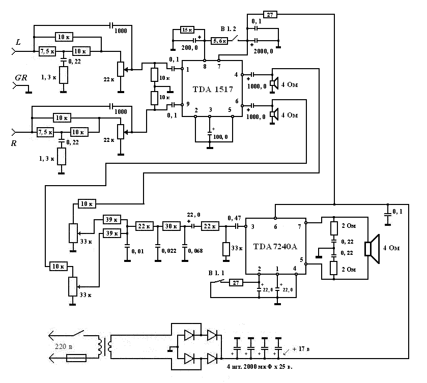
2.1 Channel Systems-Dual Power Amplifier TDA7240 and TDA1517


The main problem with the design of stereo amplifier with a total bass driver, is that the signals of left and right channels, sooner or later, are summarized. As a result of merely adding up, the separation between channels is reduced to a minimum and violated the very idea stereofonii. The most efficient method of summation, known today - signal active smesitelyami - filters with high input impedance, which is often used by field-effect transistors. Subsequent cascades enhance increase the amplitude of the signal.

I tried to make some other way - most to weaken the signals of channels and to make their addition, as late as possible, before entering signal with high sensitivity (TDA 7240 - 46dB). The second chip-TDA 1517, serves as a mid-frequency driver.

I must say that the problem is not solved completely, the separation between channels is desirable to do more, subjective listening showed a contraction of panoramas, lack of air, which is inherent in amplifiers with independent channels. Listen to music using the device somewhat tiresome, but it very effectively transmits audio material of films and computer games. In any case, the amplifier has shown significant superiority over the multimedia system Logitech Z - 340, which is one of my friends recently bought for $ 60. Another nice time - managed to realize the possibility of simultaneous volume in all channels, which will agree, very convenient. Thus, the scheme was recommended for the recurrence of 2.1 channel Systems, with the prospect of it improving.

Version 1
Version 2

Tags: 2.1 Channel Systems, Power Amplifier, Active Filter, TDA7240, TDA1517, Schematics, Electronic Circuit, Mosfet Amplifier, Audio Amplifier, Active Filter, Basic Knowledge, Basic soldering, Car Audio, Datasheet, Design, Make PCB, Modding, Power Amplifier, Power RF, Pre Amplifier, Power Supply, Loudspeaker

Power Amplifier using IC LM317


Schematic Power Amplifier using IC LM317This amplifier using IC Regulator LM317, and NPN Transistor for Gain Signal.

TDA2030 Power Amplifier Circuit


TDA2030 Power Amplifier Circuit

The TDA2030 IC is affordable and makes a good replacement amplifier for low to medium audio power systems. Incidentally, it is speaker efficiency that determines how "loud" your music is. Speaker efficiency or sound pressure level (SPL) is usually quoted in dB/meter.

A speaker with an SPL of 97dB/m will sound louder than a speaker with an SPL of 95dB/m. Although the TDA2030 can deliver 20 watts of output power, I deliberately reduced the output power to about 8 watts to supply 10 watt speakers. Input sensitivity is 200mV. Higher input levels naturally will give greater output, but no distortion should be heard. The gain is set by the 47k and 1.5k resistors.

The TDA2030 IC is affordable and makes a good replacement amplifier for low to medium audio power systems. Incidentally, it is speaker efficiency that determines how "loud" your music is. Speaker efficiency or sound pressure level (SPL) is usually quoted in dB / meter. A speaker with an SPL of 97dB / m will sound louder than a speaker with an SPL of 95dB / m.

Superb Power Amplifier using TDA7250


This 2-channel hybrid IC is normally configured with TIP142/147 power darlingtons for its' output. For those who prefer to use power transistors instead, the TDA7250 can easily be converted. All that is required are a few transistors, 4 additional resistors and some rewiring.

This conversion centers mainly on changing the output section to a Sziklai.


Sziklai Output

In our IA502 on the right, drivers Q1,Q2 are 2SC2238 and 2SA968, and outputs Q5,Q6 are 2SA1216 and 2SC2922 respectively.

No instability problems were encountered from this conversion. After a period of run-in, the amplifier remained thermally stable.

Is this version worth the extra cost and effort?


If one is only interested in something basic, the TIP version would be sufficient. But if one is after sonic performance, I would recommend this version.
http://www.ampslab.com/Images/ia502/tda7250cfp_schemahires.gif
http://www.ampslab.com/Images/ia502/tda7250cfp_components.gif


2SC2922/2SA1216 hardwired

the TDA7250 ic

Tags: Schematics, Electronic Circuit, Audio Amplifier, Design, Power Amplifier

The Design of Car Audio Power Amplifier


This article is for those who wants to make their own car amplifier. The basics of calculation will be discussed below. If you have understand it you will be able to make car amplifier yourself.

THE DESIGN OF CAR POWER AMPLIFIER

There are many designs of good amplifier published, solid state (SS) or tube designs. But few have written the design of car power amplifier

Actually the difficulty of designing the car power amplifier does not lies with the audio power amplifier, but it is more to providing the switching power supply.

As we knows, the output power of any audio power amplifier is approached by formula :

P = Vpp2/(8*Rl)

where Vpp= peak to peak supply voltage, Rl is the speaker impedance load. For car voltage of 12Vdc, if we connect it to 4 Ohm speakers we will only have power of 144/32 = 4,5 Watt. Bridging the amplifier will double the power, but will never be more than 40 W.

If we want to make more powerful amplifier, lets say 170 watt at 4 ohm speaker load, we will need supply voltage of 74Vpp, or +/- 37 Vdc. The way to have this voltage from car supply of 12VDC is to make DC-DC converter.

In this article, I will discussed the car power amplifier in 3 steps :

1. The design of audio power amplifier

2. The design of DC-DC converter

3. Miscellenous tips for making car power amplifier.

1. THE DESIGN OF AUDIO POWER AMPLIFIER

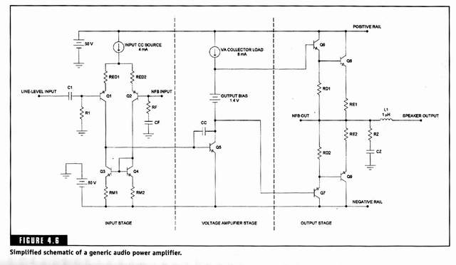
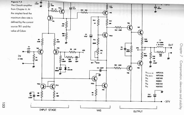
In fig1 we can see that audio power amplifier can be splitted into 3 main functions, that is:

- First stage / input stage

- Second stage / voltage amplifier stage

- Third stage / output stage

First stage is the stage that receives the input audio signal and Negative Feedback (NFB) signal from the output of the amp. Feedback is the back signal used to stabilized the audio amplifier, like the gain factor. For first stage built by discrete transistors, both signals is fed to basis of the transistor, like in fig1. Both basis of the transistors is the Non- Inverting input and Inverting Input, like those in the op-amp.

Second stage is the stage that responsibles for the Voltage Gain in the power amplifier.

Third stage is the Current Gain.

We can explain those stages in a simple way like this : Input signal, like from car radio or CD player have low voltage, about 1Vpp with few milliampere current. To produce power of 170 Watt at 4 ohm speaker load, than the signal has to have maginitude of 28Vpp and current of 6.5A (from the equation of P=I2*R = V2/R)

The first stage receives this signal in the non-inverting input and the inverting input receives NFB signal to make sure the voltage gain that the amplifier produces has a constant number, lets say 28 x. The output signal from the first stage has not reach 28Vpp, it tends to have the magnitude similiar to the input voltage. Second stage amplifies the voltage that the first stage generates. Second stage will amplifies the voltage to produce a signal that is enlarge 28x for the amplifier to have a 28Vpp signal from 1Vpp signal, but this 28Vpp signal still have small current , only a few mA and cannot drive the speaker load. The third stage amplifies the current from few mA to 6.5 A.

Offcourse the explenation for three stages above is not that simple in the real amplifier. We should take the nature's law for a transistor gain, that is G=RC/RE. This principles must be applied in each transistor in those 3 amplifier stages.

FIRST STAGE

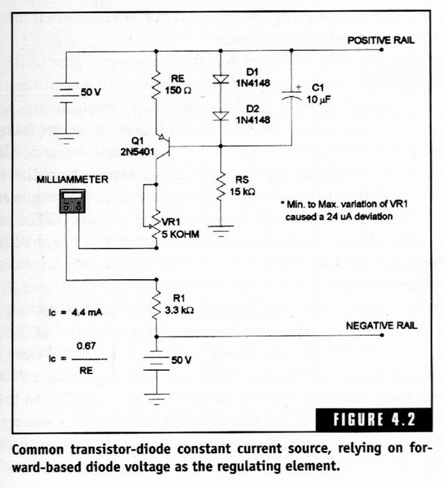
First stage designs have main component, that is Constant Current Source (CCS) which can be seen in fig2. One of the basic of electronic law that works on every circuit is that the voltage drop of Basis and Emitor (Vbe) equals the drop voltage of one dioda = 0.67V. It can be seen in fig2 that the voltage drop of 2 dioda IN4148 = 2 x 0.67V = 1,34V. We can see in RE and Q1, then V=0,67 is substracted by Vbe of Q1 and the other 0,67V will be the drop of RE. So we will have a Constant Current Source of 0,67/RE. In fig2 the Ic is = 4,4mA. CCS first stage varies between 1-4mA.

In fig1 first stage, each component will be explained like this:

- R1 is the impedance of the audio amplifier, the range is 10 Kohm – 47Kohm

- C1 is the highpass filter from the equation : Fhp = 1/(2 x pi x R1 x C1)

- RED1 and RED2 is between 50-150 ohm

- RM1 and RM2 is picked up so the voltage drop will be 50mV – 150mV

- Q3 and Q4 is the Current Mirror that ensures the current in RM1 and RM2 will have the same magnitude.

- RF and CF will be discussed later.

Before we discuss Second Stage and Third stage, first we will discuss the amplifying effect of a transistor. In fig3a we will see a circuit of Common Emitor Mode (CEM). This circuit will amplifies the voltage. In fig3b we see a Common Colector Mode (CCM). This circuit is the current amplifier without voltage amplifier. So if we want to amplifies voltage we use CEM circuit and to amplifies current we use CCM circuit.

SECOND STAGE

The Second stage responsibles for all voltage gain (Maximum Voltage Swing) in an audio power amplifier. This is why the Second stage is generally known as VAS or Voltage Amplifier Stage. This stage consist of a voltage amplifier/CEM transistor(Q5 in fig1) in the bottom, Constant Current Source in the top, and a bias control circuit in the middle. Second stage CCS has current magnitude between 4-8mA

In the second stage there is an important capacitor for an audio power amplifier , that is Miller Capacitor (CC in fig1). CC defines the pole of the frequency response for an audio amplifier and the magnitude usually in small order (severalpF).

Bias control circuit consist of a transistor, resistor and a VR like in fig5. This circuit uses a transistor that is placed in the heatsink, because the transistor have good heat compensation factor (for bipolar transistors). For the amplifier that uses mosfet transistor for the final device, the bias circuit only needs potentio or dioda only because mosfets have different heat characteristic than bipolar transistors. The bias voltage magnitude depends on the type of the third stage used, which will be discussed later.

THIRD STAGE

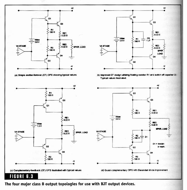
Third stage / Output Stage is the current amplifier. Third stage and the bias circuit will defines whether an amplifier works in class A, class AB or class B.

It can be said that almost 90 % of car audio power amplifier works in class B. Operation in class B does not mean that the sound produced is not good or corrupted. With good design, we will have good audio results, both from class A or class B. The choice of class B in car audio power amplifier is conected to efficiency and the heat generated. Heat generated is a very important factor, because if not considered carefully, it will lead to amplifier breakdown.

Many configurations of the output stage can be seen in fig4. Each configuration has different optimum bias voltage. It depends on how many Vbe's that have to be passed. Example : In fig4(a) the signal has to pass 4 Vbe's, which is Vbe Q1, Q3, Q4 and Q2. So the optimum bias = 4 x 0.67V = 2.8V.

Both 3 stages that we have discussed above, if we connect the together will be a circuit that can be seen in fig5. Parts of this circuit can be explained like this:

- The value of Negative Feedback (NFB) resistor is determined by determining the gain factor with the equation : Gain = 1+(R10/R8) = 1+10k/500 = 21 x. The value of R10 = value of R1 to balance input. R20 and C7 are the pole and slope compensator.

- C2 limits the DC gain factor, value ranging from 47-220 uF, usually using a nonpolar capacitor.

- R21, R22 and C11 will stabilize CCS. Here we use CCS with 2 transistor system,but the equation used still the same, that is Ic = 0,67/RE .

- The output of differential pair tapped from collector of T10 and send to VAS which is built by T12 and T4. This configuration is called Darlington VAS and the value of R8 is standard.

- C3 is the Miller capacitor with value of 100pF.

- C5 is called Speed Up Capacitor. Several designs do not use this capacitor

- R18, C6,L1 and R19 are output power stabilisator. If there is any oscilation occur in the audio power amplifier, the first tobe effected is R18 besides the final transistors.

Car Power amplifier usually loaded by low impedance speakers, usually 4 ohms and can reach ½ ohm on bridge mode. Here we know the term “High Current Amplifier”. The difference is the number of final transistors, or in fig5 it is the number of pairs of T7 and T8. As a rule of thumb, the number of transistor needed first has tobe calculated by equations above, and then we determine the number of final transistor needed with assumption that 1 transistor can handle 50 Watt output. A pair of bipolar transistor can handle 100 Watt. The power is raised by parrarelling several output transistors, so the currrent flowing will be larger. For large number of final transistors, we change the predriver stage with darlington configuration.

Several designs uses symetrical design, like those used in AXL and Crescendo schematic. this design is developed from the basic principal above, but the signal handling for + and - part is handled by complementary circuits.

I have an example about another kind of power amplifier, that is a non-feedback amplifier. You can view the principles of the "millenium power amplifier" in the www.lcaudio.com . This amplifier has a certain gain factor in first and second stage, while the third stage is only current amplifier.

2.THE DESIGN OF DC-DC CONVERTER

For building car power amplifier, we need symmetrical power supply (+, 0, -) by building DC-DC converter. The converter system discussed below will be the SMPS(Switch Mode Power Supply) type PWM (Pulse Width Modulation). This system will deliver stable output voltage, regardless of the input voltage (usually the car electrical system will range in 9-15Vdc).

To explain the SMPS type PWM, it can be analogued by the next example. Look at fig6. There is a voltage pulse V1 on-off with 50% wide. These pulses if passed through suitable L and C filter will be transformated into straight voltage of V2 which is V2 = ½ V1. (noticed the marked area below pulsed V1 is the same total area of the marked straight V2 ). With the same logic, if the pulse width of V1 is narrowed, we will have a lower V2 and if we enlarge the width of V1 pulse, we will have higher V2. Some may ask, how can we get 30VDC from the car's 12VDC? The answer is simple. If we get the V1 voltage to 60VDC, then in the 50% duty cycle, we will get 30VDC straight. This is the part where the power switching transformer takes control, to make the 60VDC from 12VDC, and then chopped by the PWM. This is the princip of PWM. (Like the principal of class D digital power amplifier). In this design, we use regulating PWM IC's, like TL494, TL594, SG3524, SG3525. These IC's will compare the output of DC-DC converter with a reference voltage. If the output of DC-DC converter is smaller than reference voltage, then the IC will enlarge the pulse width so the voltage will raise equally to to reach determined voltage. So as if the output of DC-DC converter is higher than the reference voltage, the IC will narrow the pulse width so the output voltage will be lowered to the determined voltage.

Generally SMPS used in car audio amplifier is the push-pull system with switching frequency between 20-70Khz. In push pull sytem like in fig7, Q1 and Q2 gives alternating switched current pulses so the transformator will be objected to maximum flux swing change without saturating the core.

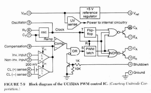
In this design we will use PWM IC with SG3524 from SGS Thompson. Specifications can be seen in SGS Thompson's website. Fig8 shows the configuration of 16 pins on this IC. To make is simpler, lets design a SMPS by explaining the function of each pin.

For the stereo power amplifier in fig5, we will need a SMPS 12Vdc input and summetrical output of +/- 37Vdc with 8A rating.

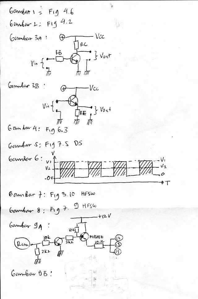
1. First we make the Remote Turn On circuit , which is connected from the car radio / CD player. The circuit can be seen in fig9a. This circuit will turn on the SMPS by giving 12Vdc to pin 12, pin 13 and pin 15.

2. The SMPS switching frequency is determined 50Khz. For this, the clock inside IC SG3524 is adjusted 2 x 50 Khz = 100Khz. This clock is built up by pin 7(Ct) and pin 6(Rt). The approach can be done with equation Fclk = 1 /(Rt x Ct). Here we use Ct = 1nF and Rt = 10Kohm like in fig9b

3. Pin 2(Non Inv In). In pin 2 we put stable reverence output for the SMPS. Here we use reference voltage of ½ from reference pin 16.

4. Pin 1(Inv In) is the output voltage detector . Pin 1 is connected to the optoisolator type 4N35 like in fig9b. Optoisolator is an important component in making this SMPS so we can have Floating Secondary Ground which will prevent noises (especially whine/storing) if the power amplifier is placed in car. The value of zener diode is 2 x 37V = 74V. If it is difficult to have zener voltage of 74 V, then we can series several zener values until we have total of 74 V.

5. Pin (4) and pin(5) are not used and connected to ground, pin(8) and pin(10) connected directly with ground.

6. Pin no 9(Comp) determines slope and pole of feedback from the whole SMPS system. In this design we use only 1 capacitor of 100nF.

7. Pin no 16(Vref) gives reverence voltage of 5,1 Vdc . This pin is placed with 10nF as a voltage stabilisator.

8. The output ripple (Vr) of the SMPS is determined by equation :

Vr = 8 x 10⁻⁶ x I / Co. With I = 8A and Vr = 0,029V we will have Co of 2.200uF in +37Vdc ->-37Vdc rail or 4400uF each in +37Vdc_0 and 4.400uF in 0_-37Vdc.

9. For output filter capacitor of 2.200uF, we will need approximately 4x 2.200uF or 8.800uF in the SMPS's input 12Vdc . The larger the value of this capacitor, more energy stored for the SMPS.

10. Output filter inductor Lo is determine by : Lo = 0,5 x Vout/ (I x F). With Vout = 2 x 37V = 74V, I = 8A dan F = 50Khz, we will have Lo = 0,092mH or Lo = 0,046mH on each supply rail + and – 37Vdc.

11. Pin 11 and pin 14 are output pins that will drive the primary winding switching mosfets. Inside IC SG3524 both pins have already opereated in mode push-pull. The circuit for driving power mosfets can be seen in fig9b. The number of power mosfet used is 3 in each transformator primary. So total there is 6 power mosfets type BUZ11.

12. Transformator(trafo) for SMPS is selfwould from ferrite toroidal core (like donuts) like in fig10. It is very important that for SMPS frequency above 20Khz, we cannot use iron core transformator like we use in homes. The ferite core transformator will have black color like in the speaker magnets, but do not have magnetizing force. The basic of equation for switching power supply with 12Vdc input is:

(1) Np = 1,37 x 10⁵ / (F x Ae), where Np= primary number of turns, F = switching frequency, Ae = X x Y = window area of ferrite in cm2. Look at fig10. To make it easy to wound the transformator, we will have to choose the toroid core with minimal diameter of 2,5 cm and window area minimal of 0.75cm2.This is necessary for the easyness of self handwound. Remember that in push-pull system there is 2 primary windings.

(2) Ns/Np = Vo/8,8, where Ns = secondary number of turns, Vo = secondary output voltage

(3) Ap = 0,004 x Vo x Io, where Ap = window area of primary wire in mm2, Vo = output voltage, Io = output current.

(4) As = 0,13 x Io, where As = window area of secondary wire in mm2.

Example : If we use toroidal ferrite core with window area of Ae = 1 cm2. then from equation no. 1 we will have number of primary turn Np = 1,37 x 10⁵ / (50Khz x 1 cm2) = 2,74 turns. In practice, number of minimal primary turns is 4 so the primary will cover the whole toroidal core. So we use 4 turns for Q1 and 4 turns for Q2.

From equation (2) we have that Ns/Np = 37/8.8 = 4,2. From here we can calculate that the number of secondary windings is = Np x Np/Ns = 4 x 4,2 = 16,8 or 17 windings. Like the primary, in secondary we use 2 x 17 turns, that is 17 turns for +37V –> 0 and 17 turns for 0-> -37V

Equation (3) is used tp determine the number of primary winding wires. We have Ap = 0,004 x 74 x 8 = 2,36mm2. If we use a 1mm diameter magnet wire, we will have window area of 0,785mm2 so we will need 3 wire magnets for each primary windings

Equation (4) is used to determine the number of wire needed for secondary windings. We have As = 0,13 x 8 = 1mm2 So if we use wire magnet with diameter of 0,8mm(window area = 0, 5mm2), then we will need 2 wires with diameter 0,8mm for each secondary windings.

13. The secondary output voltage is rectified by full bridge configuration like in fig11. Bridging diode must be the type of fast rectifier, usually looks like transistor TO220 with plate heatsink. For SMPS we cannot use ordinary 50/60Hz rectifier diode. For this design we use diode type BYW29-150, which have rating of 8A, 150V. We can also use other diodes like with prefixes FE…,MUR..., as long as it is a fast rectifier diode with minimal specification like above.

3. MISCELLENEUS TIPS FOR MAKING CAR POWER AMPLIFIER

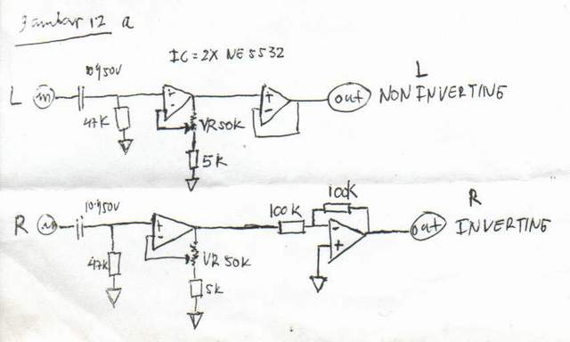
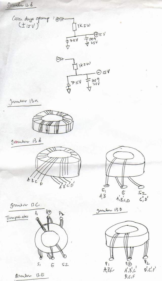
Car power amplifier has specific accesories like preamp gain circuit, an inverting channel so that the power is bridgeable. These functions usually done with opamps. The circuit can be seen in fig12a and the supply circuit can be seen in fig12b. The circuit is placed before the audio amplifier circuit.

The transformator is handwound on toroidal ferrite core. The output filter inductor can be made with ferrite core material or MPP core material. It can be made with 1.2mm wire magnet, handwound and measured until we have 0,046mH

Handwound the transformator core can be done as follow (fig13b):

- First we wound the secondary winding of 4 wires of 0.8mm magnet wires at once with 17 numbers of turn. The turn can be made in any direction as long as we consistent with the direction of the wound. If we have finished wounding it, the toroidal core will look like fig13a. We named the wires with wireA,B,C, and D. If we start the wound on top of the core, the end will be at the bottom of the core. Make sure each wire edges with AVOmeter. Connect start edge of wire A and B to point S1 and the end edge of wire A and B to point G. The start edge of wire C and D is connected to point G and the end edge of wire C and D is connected to point S2. Point G will be the secondary ground of the power amplifier and point S1 and S2 will be connected to bridging diode of BYW29.

- After we finished with secondary winding, we start to wound primary winding. Edges of primary wires is placed diagonally to the edges of the secondary wires like in fig13c. Like winding the secondary wires, we wound 6 wires of 1mm diameter at once. Name them wire A,B,C,D,E,and F. Connect the start edge of wire A,B,C to point P1 and the end edge of wire A,B,C to point P+. Connect the start point of wire D,E,F to point P+ and the end edge of wire D,E,F to point P2 (fig13d)

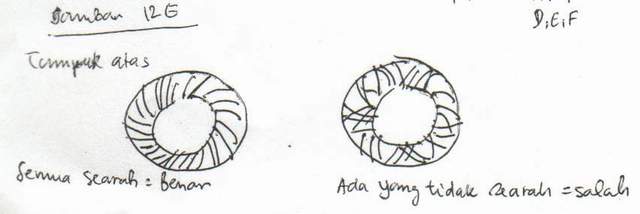
If you have finished winding the primary and the secondary, the whole transformator will have the same wire directions like in fig12e. Connect point P+ to the +12VDC of the car battery, point P1 to the drain of power mosfets Q1 and point P2 to the drain of the power mosfets Q2.

It is important to remember that all tracks in PCB layer that is connected to the power transformer has to have sufficient width due to large current will be involved. Also it is better if we soldered those tracks to have more current transfer.

After finishing winding the transformator, place all the rest of the component and finish assembly of the SMPS. You can test it by connect it with 12VDC input from the battery. Don't forget to connect the remote turn on with 12VDC. There should be output voltage of +37V, 0 and –37V without any large current draw in the 12VDC line. Check for any mistakes, if the output voltage do not present or if the SMPS draws large current from 12VDC input.

In the assembly process of car audio power amplifier, we have to pay attention in mounting all transistors to the heatsink. We must use sufficient heatsink surface so the heat won't damage the amplifier. Use mica isolator and white silicon pasta to make sure the heat transfer. Firmly tighten all the bolts to press all the transistors. Car amplifier works in vigorous environment like in the trunk of a car. Placing an extra fan always a good idea in making car power amplifier.

After we connect the SMPS to the audio amplifier, we are ready to test the car power amplifier. First trim the bias potentiometer fully left side to have minimum bias. Turn on the SMPS and look for the current draw in 12VDC line with ampmeter. The ampmeter indicator will raise for a moment to fill all the capacitors. After a few moment, the ampmeter indicator must turn back to minimum indication of ampere. If not, there is some problem. Then we trim the bias to optimal point. Usually for car stereo power amplifier total quiscent ampere will not exceed 2A of 12VDC line.

Advertisement