Showing posts with label audio amplifier. Show all posts

Very simple 18Watt Audio Amplifier Circuit project with schematic and explanation

High Quality very simple unit No need for a preamplifier.

18Watt Audio Amplifier Circuit Diagram:
18Watt Audio Amplifier-Circuit Diagram

Amplifier parts:
  
P1____22K  Log. Potentiometer (Dual-gang for stereo) 
R1___1K  1/4W Resistor 
R2___4K7 1/4W Resistor 
R3___100R  1/4W Resistor 
R4___4K7 1/4W Resistor 
R5___82K  1/4W Resistor 
R6___10R  1/2W Resistor 
R7___R22  4W Resistor (wirewound) 
R8___1K  1/2W Trimmer Cermet (optional) 
C1___470nF  63V Polyester Capacitor 
C2,C5___100µF   3V Tantalum bead Capacitors 
C3,C4___470µF  25V Electrolytic Capacitors 
C6___100nF  63V Polyester Capacitor 
D1___1N4148  75V 150mA Diode 
IC1___TLE2141C  Low noise, high voltage, high slew-rate Op-amp 
Q1___BC182  50V 100mA NPN Transistor 
Q2___BC212  50V 100mA PNP Transistor 
Q3___TIP42A  60V 6A    PNP Transistor 
Q4___TIP41A  60V 6A    NPN Transistor 
J1___RCA  audio input socket

Power supply :
Power supply  18waat a
18Watt Audio Amplifier Power Supply
Power supply parts: 
R9___2K2 1/4W Resistor 
C7,C8___4700µF 25V Electrolytic Capacitors 
D2___100V 4A Diode bridge 
D3___5mm. Red LED 
T1___220V Primary, 15 + 15V Secondary, 50VA Mains transformer 
PL1___Male Mains plug 
SW1___SPST Mains switch

Notes:
  • Can be directly connected to CD players, tuners and tape recorders.
  • Do not exceed 23 + 23V supply.
  • Q3 and Q4 must be mounted on heatsink.
  • D1 must be in thermal contact with Q1.
  • Quiescent current (best measured with an Avo-meter in series with Q3 Emitter) is not critical.
  • Adjust R3 to read a current between 20 to 30 mA with no input signal.
  • To facilitate quiescent current setting add R8 (optional).
  • A correct grounding is very important to eliminate hum and ground loops. Connect to the same point the ground sides of J1, P1, C2, C3 & C4. Connect C6 to the output ground.
  • Then connect separately the input and output grounds to the power supply ground.
Technical data: 
Output power: 
    18 Watt RMS into 8 Ohm (1KHz sine wave) 
Sensitivity: 
    150mV input for 18W output 
Frequency response: 
    30Hz to 20KHz -1dB 
Total harmonic distortion @ 1KHz: 
    0.1W 0.02% 1W 0.01% 5W 0.01% 10W 0.03% 
Total harmonic distortion @10KHz: 
    0.1W 0.04% 1W 0.05% 5W 0.06% 10W 0.15% 
Unconditionally stable on capacitive loads 

Source : RedCircuits

80 milliwatt 3 Transistor Audio Amp Circuit Schematic with explanation

This circuit is similar to the one above but uses positive feedback to get a little more amplitude to the speaker. I copied it from a small 5 transistor radio that uses a 25 ohm speaker. In the circuit above, the load resistor for the driver transistor is tied directly to the + supply. This has a disadvantage in that as the output moves positive, the drop across the 470 ohm resistor decreases which reduces the base current to the top NPN transistor. Thus the output cannot move all the way to the + supply because there wouldn't be any voltage across the 470 resistor and no base current to the NPN transistor. 

3 Transistor Audio Amp Circuit Diagram: 


80 milliwatt 3 Transistor Audio Amp Circuit Schematic with explanation


This circuit corrects the problem somewhat and allows a larger voltage swing and probably more output power, but I don't know how much without doing a lot of testing. The output still won't move more than a couple volts using small transistors since the peak current won't be more than 100mA or so into a 25 ohm load. But it's an improvement over the other circuit above.  In this circuit, the 1K load resistor is tied to the speaker so that as the output moves negative, the voltage on the 1K resistor is reduced, which aids in turning off the top NPN transistor.

When the output moves positive, the charge on the 470uF capacitor aids in turning on the top NPN transistor. The original circuit in the radio used a 300 ohm resistor where the 2 diodes are shown but I changed the resistor to 2 diodes so the amp would operate on lower voltages with less distortion. The transistors shown 2n3053 and 2n2905 are just parts I used for the other circuit above and could be smaller types. Most any small transistors can be used, but they should be capable of 100mA or more current. A 2N3904 or 2N3906 are probably a little small, but would work at low volume.

The 2 diodes generate a fairly constant bias voltage as the battery drains and reduces crossover distortion. But you should take care to insure the idle current is around 10 to 20 milliamps with no signal and the output transistors do not get hot under load.  The circuit should work with a regular 8 ohm speaker, but the output power may be somewhat less. To optimize the operation, select a resistor where the 100K is shown to set the output voltage at 1/2 the supply voltage (4.5 volts). This resistor might be anything from 50K to 700K depending on the gain of the transistor used where the 3904 is shown.

Amplificateur audio 6 watts a base de TDA2613 HI FI

6 watt audio amplifier based on TDA2613 HI FI

single scheme electronic audio amplifier 6 watt base TDA2613 HI FI: Description TDA2613: An audio amplifier circuit using 6 watts TDA2613 is shown here. TDA2613 is an integrated Hi-Fi audio amplifier IC Philips Semiconductors system. CI is ON / OFF the click proof, short-circuit, thermal protection and is available online only 9-pin plastic package. In the given circuit TDA2613 is wired to operate from a single supply. Capacitor C4 is the input DC decoupler while capacitors C5, C6 are power filters. Audio input is fed to the inverting input through capacitor C4 not. Inverting input and Vp / 2 pins of the IC are tied together and connected to ground through the capacitor C3. Capacitor C2 couples the speaker to the IC output and the network comprising capacitor C1 and resistor R1 improves the high frequency stability. Amplification Scheme 6 watts using TDA2613:


Notes:. Assemble the circuit on a good quality PCB Supply Voltage (Vs) can be between 15 to 24V DC. A heat sink is necessary to TDA2613. Do not give more than 24V TDA2613. We have over circuits audio amplifiers that may interest you: 1. 30 watts audio amplifier using TDA2040 2. Circuit 10 Watt Audio Amplifier MOSFET 3. car stereo amplifier circuit 4. Watt MOSFET amplifier circuit 50


Circuit audio amplifier TDA2040 base circuit

single electronic scheme 
Description 30 Watt audio amplifier  circuitry:. A 30-watt audio amplifier circuitry using TDA2040 is shown  here. TDA2040 is a monolithic class AB audio integrated amplifier available in Pentawatt package  The IC: has a low harmonic distortion, cross low is distortion and : has a built in protection circuitry for short circuit.  In the circuitry of two TDA2040 ICs are wired in BTL (Bridge Load tie) configuration to Provide 30W output in one 8 ohm speaker to + / -16V DC.  The capacitor C1 is the input DC decoupling capacitor.  Network comprenant components R2, C4, R3 Provides feedback to IC1 while R7, C6, R8 Network Provides information to the IC2. Network C5, C9 and R5, R9 Provides high frequency stability.  The C2, C3 filters the positive supply rail while the capacitors C7, C8 filters the negative supply rail. Single scheme electronic   circuitry diagram amplify Audio30 Watts:


Amplify audio circuit TDA2040 based system


 Notes:. A well-designed and good quality PCB Will Always Improve the sound  
 
quality. Use the + / -16V DC dual power supply to the power  
amplifier. Heat sinks are needed to IC1 and IC2  
Loads can be a speaker 8 ohms.  
C2 , C7 shoulds be Evaluated 25V electrolytic and others May be 10 or 15V.

Rangkaian Audio Amplifier TDA7295 - 80W Circuit Schematic With explanation

Rangkaian Audio Amplifier TDA7295 - 80W

The following a circuit of 80W audio amplifier is using by IC TDA7295. The circuit very simple and will be easy to build. TDA7295 has many features to support your audio system, the most important is that the IC has wide voltage range, very low distortion and very low noise feature.
Rangkaian Audio Amplifier TDA7295Rangkaian Audio Amplifier TDA7295 - 80W

TDA7295 PinningTDA7295 IC Pinning

Note:
  • The TDA7295 IC must be fitted with adequately sized heat sinks.
  • Power supply voltage should not exceed 40V
  • Connect a 50K POT in series with the input as volume control if you need. Not shown in circuit diagram.

The TDA7295 is a monolithic integrated circuit in Multiwatt 15 package, intended for use as audio class AB amplifier in Hi-Fi field applications (Home Stereo, self powered loudspeakers, Topclass TV). Thanks to the wide voltage range and to the high out current capability it is able to supply the highest power into both 4Ω and 8Ω loads even in presence of poor supply regulation, with high Supply Voltage Rejection. The built in muting function with turn on delay simplifies the remote operation avoiding switching on-off noises.

switch ON automatic cooler fan for audio amplifiers

Description.

The schematic of an automatic cooler fan for audio amplifiers is given here. The circuit automatically switch ON the cooler fan whenever the temperature of the heat sink exceeds a preset level. This circuit will save a lot of energy because the cooler fan will be OFF when the amplifier is running on low volume. At low volume less heat will be dissipated and it will not trigger the cooler fan ON.

switch ON automatic cooler fan for audio amplifiers

The temperature is sensed using an NTC (negative temperature coefficient) thermistor R2. Junction of thermistor r2 and resistor R1 is connected to the inverting input (pin3) of IC1 which is wired as a comparator. The non-inverting input (pin2) is given with a reference voltage using the preset R3. As temperature increases the resistance of NTC thermistor will drop and so do the voltage across it. When the voltage at the inverting input becomes less than that of the reference voltage (set for a particular threshold temperature) the output of the comparator goes high and switches the transistor Q1 ON. This will activate the relay and the cooler fan will be switched ON. When the temperature decreases the reverse happens. LED D2 will glow when the fan is ON. Diode D1 is a freewheeling diode.

  • The circuit can be assembled on a Vero board.
  • Use 12V DC for powering the circuit.
  • The circuit can be calibrated by adjusting the preset R3.
  • K1 can be a 12V, 200 ohm, SPST relay.
  • LM311 must be mounted on a holder.
S:circuitstoday.com

Audio amplifier circuit using TDA2822

TDA2822 is a monolithic integrated audio amplifier circuit that can be configured in stereo mode or bridge mode (BTL). The IC has low crossover distortion, low quiescent current and is available in 16 pin power DIP package. The TDA2822 can be operated from a supply voltage range of 3V to 15V. The main applications of TDA2822 are headphone amplifier, portable audio systems, mini radio, hearing aid, preamplifier etc. The IC can deliver an output power of 0.65W per channel into a 4 ohm loud speaker @ 6V supply voltage in the stereo mode and 1.35W into a

4 ohm loud speaker @ 6V supply voltage in the bridge mode.

TDA2822 stereo amplifier circuit.

TDA2822 IC configured in stereo mode is shown in fig1. The left channel input is applied to the non inverting input (pin1) of the first built in amplifier stage and the right channel input is applied to the non inverting input (pin 16) of the second built in amplifier. The inverting input of these built in amplifiers are connected to ground using separate 1000uF capacitors (C5 and C6). The amplified outputs (left and right) are available at pins 6 and 11 of the IC. The outputs are coupled to the corresponding speakers using capacitor C1 and C2 respectively. The resistor capacitor branch (0.1uF and 4.7 ohm) connected across speakers are meant for improving high frequency stability and preventing oscillations. C7 is the power supply filter capacitor.

TDA2822 amplifier circuit in bridge mode.

The output power of TDA2822 amplifier can be increased by using it in mono mode using the bridge configuration and it is shown in Fig 2. The audio input is applied to the non inverting input of the first built in amplifier. The non inverting input of the second built in amplifier is grounded. The inverting input of these amplifiers are grounded using the C9, C11 capacitor branch. Branches R5, C8 and R6, C10 are meant for improving the high frequency stability and preventing oscillations. Capacitor C12 is used for filtering the power supply.

Notes.

  • The circuit can be assembled on a Vero board.
  • The power supply can be anything between 3 to 15V DC.
  • The power supply used for this circuit must be well regulated and free from any sort of noise.
  • Optional 10K potentiometers can be added at the input lines for controlling the volume.
  • It is better to mount the TDA2822 on an IC base.

Headphone Amplifier(Class A)

Headphone Amplifier(Class A)

Description.

This is the circuit diagram of a Headphone amplifier operating in the class A push pull mode. In class A mode the output device (transistors) conduct over the entire input signal cycle. The maximum possible efficiency for Class A operation is 50% and it further reduces when capacitive coupling is used. But the advantages of Class AB amplifier are no cross over distortion, high fidelity and low harmonic distortion. These amplifiers are most suitable for low power applications.

In the circuit transistor Q1 works as the preamplifier. Resistors R6 and R7 provides potential divider biasing for Q1. Audio input is coupled to the base od Q1 through capacitor C2, resistor R9 and POT R10. Emitter of Q1 is coupled to the base of Q2 through resistor R3. Diodes D1 and D2 provides bias voltage for Q2. Base of Q3 is directly coupled to the collector of Q1. Resistor R5 limits the collector current of Q2 and Q3. C4 and C5 are power supply filter capacitors. Output of the amplifier is coupled to the head phone using the capacitor C3.

NOTES:

  • The circuit can be assembled on a vero/perf board.
  • Power supply can be anything between 6 to 24V DC.
  • I used 12V DC for powering the circuit.
  • Z1 can be a 100 ohms or higher head phone.
  • Electrolytic capacitors voltage rating must be according to the supply voltage you use.

A simple low power car stereo amplifier circuit based on TDA 2003

 A simple low power car stereo amplifier circuit based on TDA 2003

A simple low power car stereo amplifier circuit based on TDA 2003 is shown here. The circuit uses cheap, readily available components and it is very easy to construct. TDA2003 is an integrated car radio amplifier from ST Micro electronics that has a lot of good features like short circuit protection for all pins, thermal over range low harmonic distortion, low cross over distortion etc.
In the circuit given here each TDA2003 is wired as a mono amplifier operating from a 12V supply. Resistors R2 and R3 forms a feedback network that sets the amplifiers gain. C7 is the input DC de-coupling capacitor and C5 couples the speaker to the amplifiers output. C4 is used for improving the ripple rejection while C1 and C2 are employed for power supply filtering. C3 and R1 are used for setting the upper frequency cut-off. Network comprising of C6 and R4 is used for frequency stabilization and to prevent oscillation.

  • Assemble the circuit on a good quality PCB.
  • Heat sinks are necessary for both ICs.
  • The circuit can be operated from 12V DC.
  • S1 is the ON/OFF switch.
S:circuitstoday.com

MOSFET audio amplifier circuit (10 watt)


The diagram shown here is of a 10W MOSFET audio amplifier circuit that requires only a single supply. Single rail supply is seldom used in Class-B power amplifiers. Anyway, for low power applications like this it’s quite fine. Actually I got this circuit from an old cassette player that is still working and I am publishing it as it is. The powers MOSFETs BD512 and BD522 are obsolete now and so you may use any other matching power MOSFETS instead of them.
Transistors Q1 and Q2 is wired as a Darlington pair works as the preamplifier. Preset R3 controls the quiescent current while R2 provides feedback. Output is coupled to speaker through capacitor C4. Capacitor C5 is the power supply filter and C2 is the input DC decoupling capacitor.


  • The circuit can be assembled on a vero board.
  • Use 30V DC for powering the circuit.
  • Do not expect much performance from this amplifier.
  • Capacitors C3, C4, C5 must be rated 50V and C2 can be 10V.
  • Use a 8 ohm 15W speaker as load.
S:circuitstoday.com

TDA2040 based A 30 watt audio amplifier circuit

A 30 watt audio amplifier circuit using TDA2040 is shown here. TDA2040 is a Class AB monolithic integrated audio amplifier available in Pentawatt package. The IC has low harmonic distortion, low cross over distortion and has a built in circuitry for short circuit protection.

In the circuit two TDA2040 ICs are wired in BTL (Bridge Tied Load) configuration in order to deliver 30W output into an 8 ohm speaker at +/-16V DC supply. Capacitor C1 is the input DC decoupling capacitor. Network comprising of components R2, C4, R3 provides feedback for IC1 while R7, C6, R8 network provides feedback for IC2. Network C5, R5 and C9, R9 provides high frequency stability. Capacitors C2, C3 filters the positive supply rail while capacitors C7, C8 filters the negative supply rail.

TDA2040 based A 30 watt audio amplifier circuit

  • A well designed and good quality PCB will always improve sound quality.
  • Use +/-16V DC dual supply for powering the amplifier.
  • Heat sinks are necessary for IC1 and IC2.
  • Load can be an 8 ohm speaker.
  • C2, C7 must be rated 25V and other electrolytics can be 10 or 15V.
S:circuitstoday.com

TDA2613 using 6 watt audio amplifier circuit(Hi Fi)

TDA2613 using 6 watt audio amplifier circuit(Hi Fi)

A 6 watt audio amplifier circuit using TDA2613 is shown here. TDA2613 is an integrated Hi-Fi audio amplifier IC from Philips Semiconductors. The IC is switch ON / switch OFF click proof, short circuit proof, thermally protected and is available in 9 pin single in line plastic package.

In the given circuit, TDA2613 is wired to operate from a single supply. Capacitor C4 is the input DC decoupler while capacitors C5, C6 are power supply filters. Input audio is fed to the non inverting input through capacitor C4. Inverting input and Vp/2 pins of the IC are tied together and connected to ground through capacitor C3. Capacitor C2 couples the speaker to the ICs output and the network comprising of capacitor C1 and resistor R1 improves the high frequency stability.

  • Assemble the circuit on good quality PCB.
  • Supply voltage (Vs) can be anything between 15 to 24V DC.
  • Heat sink is necessary for TDA2613.
  • Do not give more than 24V to TDA2613.
S:circuitstoday.com

TDA2030 based 10W audio power amplifier


This simple 10 watts audio power amplifier is designed for home-brewed purpose. It is based on an Audio Power Amplifier IC that is called TDA2030. It is a monolithic integrated circuit in Pentawatt package, intended for use as a low frequency class AB amplifier. The TDA2030 provides high output current and has very low harmonic and cross-over distortion (0.2% at full load).

Further the circuit incorporates an original (and patented) short circuit protection system comprising an arrangement for automatically limiting the dissipated power.

S:newcircuits.com

Measured frequency response and Grado SR80 Headphones

After reading a few articles at the HeadWize forums, I got the headphone bug and figured I needed a new pair. I spent a little time researching headphones on the net, and the Grado line of headphones, particularly the SR60 and SR80 were getting good reviews relative to their cost..

Grado SR80 Headphones
So I went headed off to the local Hi-Fi shop and gave a few "cans" a good listen. I did not want to break the bank, so I concentrated on the Grado line of headphones. I listened to the SR60, SR80, SR125 and SR225. As one would expect, they generally got better as you moved up the line. The SR60s seems to have the best bass of the bunch, but seemed a little dry in the midrange. To my ears, the differences between the SR80 and the SR125/SR225 were subtle, so I went with the SR80. If you prefer music with more of a thump, the SR60 are an excellent choice and also the lowest cost of the bunch.

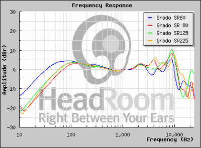
A comparison of the measured frequency response (by headphone.com) is shown in the plot below.

Grado SR60 / SR80 / SR125 / SR225 Headphone Frequency Response Plot

Lower cost CMoy Mint Tin Headphone Amplifier


A while back I purchased a nice pair of cans ... Grado SR80 Headphones. When I bought them, I knew that they would drive me to build a DIY headphone amplifier. Well, here are the results ... A very simple CMoy mint tin headphone amplifier.

Grado SR80 Headphone and CMoy Amplifier
The CMoy is a very popular and easy to build headphone amplifier that can be fit into a mint tin. It can be used to drive demanding headphones, produce thunderous volumes and most importantly, it sounds excellent. The original article A Pocket Headphone Amplifier by Chu Moy discusses all the fine points of the amplifier, while How to Build the CMoy Pocket Amplifier provides excellent and easy to follow building instructions.

My version of the CMoy headphone amplifier uses two nine volt batteries, the OPA2132PA (Burr-Brown) operational amplifier (opamp) and I originally set the gain to 9 - which turned out to be far too high. I have since adjusted the gain down to about 3. Since I will be using this with a portable MP3 player, I elected not to include a potentiometer as the volume will be controlled through the MP3 player.

CMoy Headphone Amplifier in Altoids Mint Tin
The CMoy headphone amplifier sounds pretty darn good when you consider the simplicity and low cost. It provides excellent clarity, even at high volume. The headphone amplifier does not seem to add its own colorations to the sound and there is a lot of detail. The amplifier is very well behaved and there are no pops when powering up or hiss during operation. Overall, this is a very nice little performer and it considerably increases listening pleasure with a good set of headphones.

(gainclone) LM3886 Chip Amplifier


LM3886 ChipAmp (gainclone)

After several months of planning and acquiring parts, I finally got down to constructing a chip amp (gainclone). The amp uses the National Semiconductor LM3886 chip with printed circuit boards (PCB) purchased from chipamp.com. I finished the amp late last night, so I only have about 3 hours on it and I don’t think it is burnt in. So far it sounds pretty good. It sounds much better than it should given the simplicity and low cost of this amp. There is a lot of power available and the bottom end is very good.

Non-Inverting Chip Amplifier using the LM3875 kits

Bruce has put together a LM3875 based Non-Inverting Chip Amplifier using the LM3875 kits available from audiosector.com. He has affectionately named his project the "Beast". For the enclosure, Bruce used plastic and aluminum project boxes from Radio Shack. The power supply consists of a 200VA toroidal transformer and is housed in a separate enclosure.

LM3875 DIY Chipamp Kit
Consistent with what most are chip amp kit builders have been finding out, Bruce has found out that these gainclone kits result in a great sounding amplifier at a reasonably low cost..

Oatley Electronics K282 Tube Based Stereo RIAA Preamplifier Kits

Last year Mark built a number of the Oatley Electronics K272 tube headphone amp kits and he has recently got his hands on the new Oatley Electronics K282 Tube Based Stereo RIAA Preamplifier Kits. The kit is for moving magnet (MM) cartridges. The inexpensive kit costs $47AU (about $44US, $44CDN, $33EU, 29GBP) and includes a power supply.


Like the headphone amplifier kit, the phono preamp kit is based around new old stock (NOS) Raytheon JAN 6418 sub-miniature pentode tubes. The circuit is a tube hybrid with FET stages and a SMPS.


The kit is built on a through-hole PCB and also includes a "universal" 5V power supply that will operate pretty much everywhere. You will have to provide your own audio connections (RCA jacks) and an enclosure. As Mark notes, for best performance you will need to pay special attention to controlling vibration and mechanical noises as the sub-miniature tubes are extremely microphonic.


Mark reports that the inexpensive kit is a good performer. With the low cost of the kit, this is a great low voltage kit for those interested in tube or phono audio.

Audio power amplifier with mute


The LM3876 is a high-performance audio power amplifier capable of delivering 56W of continuous average power to an 8 load with 0.1% THD+N from 20Hz-20kHz.The performance of the LM3876, utilizing its Self Peak Instantaneous Temperature protection circuitry, puts it in a class above discrete and hybrid amplifiers by providing an inherently, dynamically protected Safe Operating Area. SPiKer protection means that these parts are completely safeguarded at the output against overvoltage, undervoltage, overloads, including shorts to the supplies, thermal runaway, and instantaneous temperature peaks.The LM3876 maintains an excellent signal-to-noise ratio of greater than 95dB (min) with a typical low noise floor of 2.0µV. It exhibits extremely low THD+N values of 0.06% at the rated output into the rated load over the audio spectrum, and provides excellent linearity with an typical rating of 0.004%.


Features


56W continuous average output power into 8Ω
100W instantaneous peak output power capability

Signal-to-Noise Ratio >= 95 dB(min)

An input mute function

Output protection from a short to ground or to the supplies via internal current limiting circuitry

Output over-voltage protection against transients from inductive loads

Supply under-voltage protection, not allowing internal biasing to occur when VEE + VCC <= 12V, thus eliminating turn-on and turn-off transients

11-lead TO-220 package

Wide supply range 20V - 94V


Part list

Resistor:
R1, R3 = 1 k
R2, R4, R5 = 18k
R6 = see text
R7 = 10R, 5 Watt
R8, R9 = 22k
Capacitors:
C1 = 2.2 uF
C2 = 220 uF, 160 V
C3 = 22 uF, 40 V
C4 = 47 pF
C5 = 100 uF, 40 V
C6 = see text
C7, C8 = 100 nF
C9, C10 = 1000 uF, 40 V
Inductors:
L1 = 0.7 uH – see text
Integrated circuits:
IC1 =
LM3876T

Miscellaneous:Heat sink for IC1
Air-cored inductor L1 consists of 13 turns of 1mm dia. enamelled copper wire with an inner diameter of 10mm. The completed inductor is pushed over R7 and its terminals soldered to those of the resistor.All electrolytic capacitors must be mounted upright. The amplifier can be muted with a single-pole switch connected to the MUTE input (pin8). This function is enabled when the switch is open. If muting is not required, solder a wire bridge across the mute terminals on the board. Boucherot network R6-C6 is not normally required in this application, but provision has been made for it for use in other applications. According to the manufacturers, both chips are optimalized for a load of 8 Ohm. The output power is lower when a 4 Ohm load is used or when the supply voltage is reduced. When a 4 Ohm load is used, the SPIKE protection becomes active when the supply voltage is about 27V, resulting a in a reduction of the power output to 10W. This means that it is not advisable to use loudspeaker with an

Technical data for Amplifier(30w) used in cars


The power that can be obtained from a standard car radio amplifier operating from a 12 V car battery is 5–6W, which (for many listeners) is not really enough for satisfactory hi-fi reproduction. It is, of course, possible to boost the 12 V supply with a power inverter, but that is fairly expensive and not always acceptable. Now, a Philips IC enables audio power of about 30 W to be obtained from a 12 V car battery

Technical Data
Class H operation
Low dissipation with music signals
Extensive protection circuits (output current; temperature; load impedance)
Supply voltage 12 V nominal
Quiescent current 100 mA
Output power
(1 kHz sinusoidal, THD = 0.5%) 30 W r.m.s. into 8 Ω
(music signal) 40 W into 8 Ω
THD + noise (1 W into 8 Ω = 0.05% (20 Hz to 20 kHz)
THD + noise (20 W into 8 Ω = 0.2% (20 Hz to 20 kHz)
Power bandwidth (–3 dB) 5 Hz to 100 kHz

Advertisement