
This small circuit is a Linear amplifier for driving small UHF TV transmitters. Its gain is 7dB and can amplify a signal between 450-800 MHz. You can drive the circuit with 1 to 1,5 Watts signal. Better use double layer PCB with the second layer connected to earth. Use a stabilized power supply 25 volts and at least 5Amps.
Source: http://www.next.gr/inside-circuits/5-Watt-UHF-TV-Linear-amplifier-l4899.html
UHF TV Linear amplifier 5 W by BLW98
UHF TV linear amplifier 4W by BF136
a

That Circuit is a UHF TV linear amplifier for small TV transmitters with output aroun 100-200mW. The transistor BGQ136 comes with SOT-122 case has gain of 13dB at 800MHz. So with input 100mW you get 2W output and for 200mW you get 4W.
Read Source: http://www.next.gr/inside-circuits/4Watt-UHF-TV-linear-amplifier-l4360.html
HF 300KHz-30Mhz Linear Amplifier

This is a rather unusual QRP Power Amplifier design, with a wide frequency response; within three dB’s from 300KHz to 30MHz. Overall gain is in the region of 16dB and the final output power may be well over four watts. This PA will deliver 4 watts continuously (with a suitable heatsink), and may be loaded into a short-circuit or open circuit without causing damage. This makes it almost the ideal PA for outdoor/field use. Above is the full circuit diagram of the RFPA and the coil winding pattern. This PA may be used for for SSB, [...]
Read more source:
http://w1.859.telia.com/~u85920178/tx/linear.htm
XTR106: 4-20mA Current Transmitter with Bridge Excitation And Linearization
The XTR106 is a low cost, monolithic 4-20mA, two-wire current transmitter designed for bridge sensors. It provides complete bridge excitation (2.5V or 5V reference), instrumentation amplifier, sensor linearization, and current output circuitry. Current for powering additional external input circuitry is available from the VREG pin.
The instrumentation amplifier can be used over a wide range of gain, accommodating a variety of input signal types and sensors. Total unadjusted error of the complete current transmitter, including the linearized bridge, is low enough to permit use without adjustment in many applications. The XTR106 operates on loop power supply voltages down to 7.5V.
Linearization circuitry provides second-order correction to the transfer function by controlling bridge excitation voltage. It provides up to a 20:1 improvement in nonlinearity, even with low cost transducers.
&The XTR106 is available in 14-pin plastic DIP and SO-14 surface-mount packages and is specified for the –40°C to +85°C temperature range. Operation is from –55°C to +125°C.
Source: http://focus.ti.com/docs/prod/folders/print/xtr106.html
12 Volt Fluorescent Lamp 20W Drivers

Here is the schematic diagram for a 20 Watt driver. I developed this circuit in 1985, and used it to build a lamp that found much use both as camping light and as emergency light during the then-frequent power outages.
Buy Fluorescent Lamp Driver
BUY 12V Fluorescent Lights
The two transistors work as a push-pull oscillator. To avoid crossover conduction, during operation the bases are self-biased to a slightly negative voltage by the 1R5 resistor. The 220uF capacitor gives strong positive bias during power-up, in order to get the oscillator started. 2k2 resistors only purpose is discharging the capacitor when the circuit is switched off, so it will restart the next time too!
Source:http://ludens.cl/Electron/Fluolamp/fluolamp.html
Thank you
Pulse-Generator & Signal-Tracer with BC547,BC557
Dual-purpose test-instrument
Very simple circuitry, 1.5V Battery-operated

Parts:
R1__________________1M 1/4W Resistor
R2,R4_______________2K7 1/4W Resistors
R3________________150K 1/4W Resistor
C1__________________2n2 630V Ceramic or Polyester Capacitor (See Notes)
C2,C3_______________4n7 63V Ceramic or Polyester Capacitors
D1_______________1N4148 75V 150mA Diode
Q1________________BC547 45V 100mA NPN Transistor
Q2________________BC557 45V 100mA PNP Transistor
SW1________________SPST miniature Slider Switch (See Notes)
J1_________________Stereo switched 3mm. Jack socket (See Notes)
Probe______________Metal Probe 3 to 5 cm. long
Clip_______________Miniature Crocodile Clip
B1_________________1.5V Battery (AA or AAA cell etc.)
Related Links
More circuit about Meter
More circuit about Pulse Generator
More circuit about Oscillator Generator
More circuit about Squarewave Oscillator
Squarewave Oscillator by IC LM339
XR2206 Function Generator.
8038 Tri-Waveform Generator (Easy Oscillator Generator)
Triangle and Squarewave Generator
Function Generator by IC 1458
32.768 KHz oscillator using a watch crystal
Cmos Logic Clock Oscillator by Ic 4011
X’tal Oscillator Frequency by 74LS04
Read More Source:
http://www.redcircuits.com//Page59.htm
Start System Thinking
How we think influences human's behaviour everyday. Russell L. Ackoff, a philosopher, thinks that traditionally scientific system thinkings are based on two main ideas.
First idea is based on understanding about every phenomenon can be explained with cause-effect corelation which says that every thing has a cause if the cause is necessary and sufficient. This system thinking is not enough, because it's often impossible for us to find the cause-effect corelation for every component in the system.
Second idea called reductionist which stated that everything in this world (and every experience about the world) can be reduced, decomposed, disassemblied or divided until it becomes parts that can't be divided anymore. The problem solution for every part is assumed to be able to solve the whole problem.
Let's see some examples which are rather extreme:
1. A father has problems with diabetes and liver. To solve this problem, his son divide this problem into two parts, which is diabetes and liver. One day, his son took him to a doctor to cure his diabetes to solve the first part (the first problem). Another day, his son took him to another doctor to cure his liver to solve the second part (the second problem). Both doctors surely gave different presriptions. The diabetes doctor gave him medicines to lower glucose level in his blood, another doctor gave him other medicines to increase glucose level in his blood so his liver can work again.
In this problem, mistakes was done by all parties, why both the son and the father did not tell the doctors about the father's whole problem and why the doctor did not ask what medicines is being consumed by the father. Maybe that's the result of reductionist system thinking.
2. When we do an essay test, a problem may not consist only one question, there may be some questions, it's better if we read the all questions that are related to the question first then answer the questions, because it often happens when we answer the question one by one, when we do the next question, that time we may just really understand what the examiners want.
3. This is a more common example, when we translate sentences from one language to another, if we translate the word one by one without seeing the sentence context, then assembling it, the result is not impossibly becoming weird.
4. I watched a movie about an otaku. He loves a girl. But one day, his friends ask him to see an exebition called "Comixet". He told the girl that he has to work but actually he came to see the exebition, having fun with his friends in his otaku dress. But, suddenly he met the girl, the girl saw him in his otaku dress then she told him not to meet her again. He think it is his fault that he is an otaku. He throw away all his toys; gundams, models, comics, etc. Then he told the girl that he has left his otaku behaviour, but the girl still can't forgive him. Actually, he is an otaku, that is not a problem, the main problem is his small lie. How the story continues... watch "Densha Otoko"!
So, that's why that kind of system thinking is considered left behind. In the present times, when we have a problem, we should not think like our ancestor did, because many problems may not be possible to be solved by those two, the better idea is thinking with "system thinking", so we think to get a solution for the whole problem, not by its parts.
source : kejut.com
Ceramic Sintering
Sintering is a method for making objects from powder, by heating the material in a sintering furnace below its melting point (solid state sintering) until its particles adhere to each other. Sintering is traditionally used for manufacturing ceramic objects, and has also found uses in such fields as powder metallurgy.
The word "sinter" comes from the Middle High German Sinter, a cognate of English "cinder".
Sintering is part of the firing process used in the manufacture of pottery and other ceramic objects. Some ceramic raw materials have a lower affinity for water and a lower plasticity index than clay, requiring organic additives in the stages before sintering. The general procedure of creating ceramic objects via sintering of powders includes:
* Mixing water, binder, deflocculant, and unfired ceramic powder to form a slurry
* Spray-drying the slurry
* Putting the spray dried powder into a mold and pressing it to form a green body (an unsintered ceramic item)
* Heating the green body at low temperature to burn off the binder
* Sintering at a high temperature to fuse the ceramic particles together
All the characteristic temperatures associated to phases transformation, glass transitions and melting points, occurring during a sinterisation cycle of a particular ceramics formulation (i.e. tails and frits) can be easily obtained by observing the expansion-temperature curves during optical dilatometer thermal analysis. In fact, sinterisation is associated to a remarkable shrinkage of the material because glass phases flow, once their transition temperature is reached, and start consolidating the powdery structure and considerably reducing the porosity of the material.
There are two types of sintering: with pressure (also known as hot pressing), and without pressure. Pressureless sintering is possible with graded metal-ceramic composites, with a nanoparticle sintering aid and bulk molding technology. A variant used for 3D shapes is called hot isostatic pressing.
To allow efficient stacking of product in the furnace during sintering and prevent parts sticking together, many manufacturers separate ware using Ceramic Powder Separator Sheets. These sheets are available in various materials such as alumina, zirconia and magnesia. They are also available in fine medium and coarse particle sizes. By matching the material and particle size to the ware being sintered, surface damage and contamination can be reduced while maximizing furnace loading.
source : www.wikipedia.org
Wireles LAN TL-WR941ND-300Mbps Wireless N Router
 The TL-WR941ND Wireless N Router is a combined wired/wireless network connection device designed specifically for small business, office, and home office networking requirements. It complies with the IEEE 802.11n standard with wireless transmission speeds of up to 300M. The router features 4 10/100Mbps ports to achieve the most effective data transmission. It adopts MIMO, has three detachable Omni directional antennas providing even better wireless performance, transmission rates, stability and coverage. CCA™ technology automatically avoids channel conflicts using its channel selection feature. It also works well with other 11g and 11n protocol wireless products.
Features
- Supports PPPoE, Dynamic IP, and static IP broadband functions
- Automatic dialing, On-demand dialing, detachable time dialing, filling most dialing requirements
- Supports UPnP, DDNS, static routing, VPN Pass-through
- Supports virtual server, special application and DMZ host ideal for creating a website within your LAN
- Supports SSID broadcast control and MAC access control list
- Supports 64/128/152-bit WEP, complies with 128 bit WPA standard(TKIP/AES), supports MIC, IV Expansion, Shared Key Authentication, IEEE 802.1X
- Built-in firewall features IP, MAC, URL filtering which flexibly controls online access and time
- Built-in DHCP server with automatic dynamic IP address distribution
- User interface supports free WEB software updates
- Supports configuration file backup and restore
- 3 detachable Omni directional antennas
- Sleek exterior, can be mounted on a wall or placed horizontally on a table or desk
Software Specification | |
| Standards | IEEE 802.11n, IEEE 802.11g, IEEE 802.11b |
| Wireless Signal Rates With Automatic Fallback | 11n: Up to 300Mbps(dynamic) 11g: Up to 54Mbps(dynamic) 11b: Up to 11Mbps(dynamic) |
| Frequency Range | 2.4-2.4835GHz |
| Wireless Transmit Power (MAX) | 20dBm (max. EIRP) |
| Modulation Technology | DBPSK, DQPSK, CCK, OFDM, 16-QAM, 64-QAM |
| Receiver Sensitivity | 270M: -68dBm@10% PER 130M: -68dBm@10% PER 108M: -68dBm@10% PER 54M: -68dBm@10% PER 11M: -85dBm@8% PER 6M: -88dBm@10% PER 1M: -90dBm@8% PER |
| Hardware Specification | |
| Interface | 4 10/100M LAN Ports 1 10/100M WAN Port |
| Antenna | 3dBi Detachable Omni Directional Antenna X 3 |
| Power Supply Unit | Input: Localized to Country of Sale Output: 9VDC / 0.85A Switching PSU |
| Operating temperature | 0oC~40oC(32oF~104oF) |
| Storage temperature | -40oC~70oC (-40oF~158oF) |
| Relative humidity | 10% ~ 90%, Non Condensation |
| Storage Humidity | 5%~95% Non-Condensing |
| Dimensions | 7.9 x 5.5 x 1.2 in. (200 x 140 x 28mm) |
Source : tp-link.com
The Advantages and Disadvantages of Air lift Bioreactor
1. Simple design with no moving parts or agitator for less maintenance, less risk of defects.
2. Easier sterilization (no agitator shaft parts)
3. Low Energy requirement vs stirred tank
Obviously doesn’t need the energy for the moving parts (agitator shaft).
4. Greater heat-removal vs stirred tank
At the Airlift bioreactor it doesn’t need the heat plate to control the temperature, because the Draught-Tube which is inside the bioreactor can be designed to serve as internal heat exchanger. It is difference to the Stirred tank bioreactor that needs the heat coat or plate surrounding the tank to make warm bioreactor. It is clear enough that the Airlift bioreactor has greater heat-removal compare to Stirred tank.
The Disadvantages of Airlift Bioreactor:
1. Greater air throughput and higher pressures needed
The agitation on the Airlift bioreactor is controlled by the supply air. To adjust the supply air then the higher pressure needed. And if the higher pressure of air needed then more energy consumption needed. And more cost must pay.
2. Inefficient break the foam when foaming occurs
Because there is no blades/shaft as a foam breaker compare with the stirred tank that has it at the surface.
3. NO bubbles breaker
There are no blades that used as a breaker the bubbles which produced from the air supply (sparger)
Wireles LAN TL-WR1043ND-Ultimate Wireless N Gigabit Router

The TP-LINK Wireless N Gigabit Router TL-WR1043ND is a combined wired/wireless network connection device integrated with internet-sharing router and 4-port Gigabit switch. Adopting advanced MIMO™ (Multi Input Multi Output) and SST™ technologies, it provides incredibly high wireless speeds of up to 300Mbps. The TL-WR1043ND also features four Gigabit Ethernet ports for wired connections. This robust guaranteed wired/wireless throughput ensures that you are freer to simultaneously enjoy multiple high-bandwidth consuming and interruption sensitive applications such as streaming HD video, making VoIP calls, sharing large files and playing online games. The TL-WR1043ND is specially equipped with a USB storage port on the back of the router for connecting USB storage devices, for convenient access for everyone on the network.
*Some official firmware of TP-LINK products can be replaced by the third party firmware such as DD-WRT. TP-LINK does not provide technical support and does not guarantee the performance and stability of third party firmware. Damage to the product as a result of using third party firmware will void the product's warranty.
Features
- Gigabit Ethernet ports enabling ultimate transfer speed
- Centrally storing and content sharing by connecting USB storage drives
- SST™ dramatically increases link robustness and stability
- CCA™ improves wireless performance while automatically avoiding channel conflicts
- Wireless N speed up to 300Mbps makes it ideal for bandwidth consuming or interruption sensitive applications like video streaming, online gaming and VoIP
- For home and office use, supports PPPoE, Dynamic IP, and static IP broadband access and various kind of dialing requirements
- Supports UPnP, DDNS, static routing, VPN pass-through, and data forwarding
- Features IP, MAC, URL filtering which flexibly controls online access and time
- Supports SPI firewall and access control management
- Supports QSS (Quick Secure Setup), provides 64/128/152-bit WEP encryption, WPA/WPA2, WPA-PSK/WPA2-PSK authentication
- User interface supports free web software updates
- 3 detachable antennas (reverse SMA connector)
Specification
Software Specification | |
| Standards | IEEE 802.11n, IEEE 802.11g, IEEE 802.11b |
| Wireless Signal Rates With Automatic Fallback | 11n: Up to 300Mbps(dynamic) 11g: Up to 54Mbps(dynamic) 11b: Up to 11Mbps(dynamic) |
| Frequency Range | 2.4-2.4835GHz |
| Wireless Transmit Power (MAX) | 20dBm(Max. EIRP) |
| Modulation Technology | DBPSK, DQPSK, CCK, OFDM, 16-QAM, 64-QAM |
| Receiver Sensitivity | 270M: -68dBm@10% PER 130M: -68dBm@10% PER 108M: -68dBm@10% PER 54M: -68dBm@10% PER 11M: -85dBm@8% PER 6M: -88dBm@10% PER 1M: -90dBm@8% PER |
| Hardware Specification | |
| Interface | 4 10/100/1000M LAN Ports 1 10/100/1000M WAN Port 1 USB 2.0 Port |
| Antenna | 3dBi Detachable Omni Directional Antenna X 3 |
| Power Supply Unit | Input: Localized to Country of Sale Output: 12VDC / 1.5A Switching PSU |
| Operating temperature | 0oC~40oC (32oF~104oF) |
| Storage temperature | -40oC~70oC(-40oF~158oF) |
| Relative humidity | 10% ~ 90%, Non-Condensing |
| Storage Humidity | 5%~95% Non-Condensing |
| Dimensions | 7.9 x 5.5 x 1.2 in. (200 x 140 x 28mm) |
source : tp-link.com
The Newest Processor : Intel Core i7

Intel Corporation (NASDAQ: INTC; SEHK: 4335; Euronext: INCO) is the inventor of the x86 series of microprocessors, the processors found in most personal computers. The company is the world's largest semiconductor chip maker, based on revenue. Intel was founded on July 18, 1968, as Integrated Electronics Corporation (though a common misconception is that "Intel" is from the word intelligence) and is based in Santa Clara, California, USA. Intel also makes motherboard chipsets, network interface controllers and integrated circuits, flash memory, graphic chips, embedded processors, and other devices related to communications and computing. Founded by semiconductor pioneers Robert Noyce and Gordon Moore, and widely associated with the executive leadership and vision of Andrew Grove, Intel combines advanced chip design capability with a leading-edge manufacturing capability. Originally known primarily to engineers and technologists, Intel's "Intel Inside" advertising campaign of the 1990s made it and its Pentium processor household names.
Intel was an early developer of SRAM and DRAM memory chips, and this represented the majority of its business until the early 1980s. While Intel created the first commercial microprocessor chip in 1971, it was not until the success of the personal computer (PC) that this became their primary business. During the 1990s, Intel invested heavily in new microprocessor designs fostering the rapid growth of the PC industry. During this period Intel became the dominant supplier of microprocessors for PCs, and was known for aggressive and sometimes controversial tactics in defense of its market position, particularly against AMD, as well as a struggle with Microsoft for control over the direction of the PC industry. The 2009 rankings of the world's 100 most powerful brands published by Millward Brown Optimor showed the company's brand value rising 4 places – from number 27 to number 23.
Processor Intel Core i7
Intel Core i7 is Intel's brand name for several families of desktop and laptop 64-bit x86-64 processors using the Intel Nehalem microarchitecture.
It is a successor to the Intel Core 2 brand. The Core i7 identifier was first applied to the initial family of processors codenamed Bloomfield introduced in 2008. In 2009 the name was applied to Lynnfield and Clarksfield models. Prior to 2010, all models were quad-core processors. In 2010, the name was applied to dual-core Arrandale models, and the Gulftown Core i7-980X Extreme processor which has six hyperthreaded cores.
Intel representatives state that the moniker Core i7 is meant to help consumers decide which processor to purchase as the newer Nehalem-based products are released in the future.[8] The name continues the use of the Intel Core brand. Core i7, first assembled in Costa Rica, was officially launched on November 17, 2008[11] and is manufactured in Arizona, New Mexico and Oregon, though the Oregon (PTD, Fab D1D) plant has already moved to the next generation 32 nm process.
Processor Cores
The initial Core i7 processors released were codenamed Bloomfield, branded as Core i7-9xx along with their Xeon 3500-series counterparts. As of 2009, they are Intel's high-end Desktop processors, sharing the Socket 1366 platform with the single and dual-processor server processors.
Lynnfield is the second processor sold under the Core i7 brand, while at the same time being sold as Core i5. Unlike Bloomfield, it does not have a QPI interface but directly connects to a southbridge using a 2.5 GT/s Direct Media Interface and to other devices using PCI Express links in its Socket 1156. Core i7 processors based on Lynnfield have Hyper-Threading, which is disabled in Lynnfield-based Core i5 processors.
Clarksfield is the mobile version of Lynnfield and available under the Core i7 Mobile brand, as part of the Calpella platform. It was released at the Intel Developer Forum on September 23, 2009.
The second mobile Core i7 processor family will be Arrandale, sold as the Core i7-6xx processors and featuring an integrated graphics processing unit but only two processor cores, half of Clarksfield. Clarkdale, the desktop version of Arrandale, will not be sold as Core i7, but only as Core i3 and Core i5. All support Intels Hyper Threading (HT).
Gulftown is the Extreme Edition version of the Core i7, featuring 6 cores, 32nm process, Hyper-Threading (for a total of 12 logical threads), 12 MB of cache, Turbo Boost and Intel QuickPath connection bus
ref : wikipedia
Pharm-D course to be offered in six colleges HYDERABAD: The much awaited Pharm-D course will be offered in six colleges in the State this year and t
Pharm-D course to be offered in six colleges
HYDERABAD: The much awaited Pharm-D course will be offered in six colleges in the State this year and the State Government issued the necessary orders on Tuesday. The orders were issued after the Pharmacy Council of India (PCI) gave its nod considering all aspects.
Permission was given to St. Peter’s Institute of Pharmaceutical Sciences, Hanamkonda, Deccan School of Pharmacy, Hyderabad, Talla Padmavathi College of Pharmacy, Warangal, Sarojini Ramulamma College of Pharmacy, Mahabubnagar; Raghavendra Institute of Pharmaceutical Education & Research, Anantapur, and Sri Venkateshwara College of Pharmacy, Hyderabad. All the colleges will have an intake of 30 seats each.
The Government orders said that the admissions would be taken up as per the guidelines issued in G.O. 61 and the colleges have to get affiliation from the concerned universities. The A.P. Private Pharmacy Colleges’ Managements Association has said that entry for the six-year course would be based on Intermediate marks. T. Jayapal Reddy, general secretary and K. Ramdass, treasurer in a statement said that admissions would be completed by the month-end. The Pharm-D course allows students to practice in the USA and the West after clearing the concerned examinations there. The B. Pharmacy four-year course has some limitations for students planning to go abroad.
The Distance Transform of a Binary Image This is a image processing program which performs the distance transform of a binary image.Distance transfo
The Distance Transform of a Binary Image
This is a image processing program which performs the distance transform of a binary image.Distance transform is widely used for image thinning and finding skeleton of an image.
//1:newfndistrans.java
//2:A bmp monochrome image(preferably 512-512)
//make the image from mspaint or any other source
import java.io.*;
import javax.swing.*;
import java.awt.*;
import java.awt.event.*;
public class newfndistrans extends JFrame{
frame frm=null;
File f;
FileInputStream ff;
Color cl;
int count;
int a[];
int rnum,gnum;
int xsize;
int ysize;
final int sample=5;
String str=null;
newfndistrans(String str)
{
super(str);
frm=new frame();
count=0;
a=new int[8];
rnum=0;gnum=0;
}
public void paint(Graphics g)
{
int x,y,i=0,j=0,temp;
try{
System.out.println("Starting");
System.out.println("filename="+frm.getfilename());
try{f=frm.getfilename();
ff=new FileInputStream(f);
}catch(Exception e){
System.out.println("error in reading file");
}
ff.skip(18);
i=ff.read();
i=((ff.read()<<8 i="((ff.read()<<16" i="((ff.read()<<24" xsize="i;" width="+xsize); i=0; i=ff.read(); i=((ff.read()<<8 )|i ); i=((ff.read()<<16 )|i ); i=((ff.read()<<24 )|i ); ysize=i; System.out.println(" height="+ysize); ff.skip(38);//62-(2+16+4+4=26)=36, actually total=62 Bytes header //note:make it 38 for nrectbit1.bmp and nrectbit2.bmp x=0;y=ysize; int pix[][],mat1[][]; pix=new int[xsize][ysize]; mat1=new int[xsize][ysize]; System.out.println(" rnum="ff.read();" rnum="" rnum="="-1)break;" count="7;">0)
{
gnum=rnum%2;
if(gnum==0)a[count]=1;
else a[count]=0;
count--;
rnum=rnum/2;
}
while(count>=0)
{a[count]=1;count--;
}
for(i=0;i<=7;i++) {if(a==0)cl=new Color(255,255,255);
else cl=new Color(0,0,0);
pix
mat1
g.setColor(cl);
g.drawRect(x,y,1,1);
x++;
if(x==xsize){x=0;y--;}
}
}//end while
System.out.println("File read successfully");
//sleep for 4 seconds(4000 msec)
try{Thread.sleep(4000);
}catch(Exception e){}
//clear the region where the image was drawn,area near the boundaries
are
also cleaned
for(j=0;j<=ysize+2;j++) for(i=0;i<=xsize+2;i++) g.clearRect(i,j,1,1); //cleaning done above //0 means white,1 means black //perform the distance transform for(j=0;j[j]==0)continue;
if((j==0)||(j==ysize-1)){mat1[j]=1;continue;}
if((i==0)||(i==xsize-1)){mat1[j]=1;continue;}
temp=findmin(mat1[i-1][j],mat1[i-1][j-1],mat1[j-1],mat1[i+1][j-1]);
mat1[j]=temp+1;
}
//perform the distance transform from bottom
for(j=ysize-1;j>=0;j--)
for(i=xsize-1;i>=0;i--)
{if(mat1[j]==0)continue;
if((j==0)||(j==ysize-1)){mat1[j]=1;continue;}
if((i==0)||(i==xsize-1)){mat1[j]=1;continue;}
temp=findmin(mat1[i-1][j+1],mat1[j+1],mat1[i+1][j+1],mat1[i+1][j]);
if(temp>(mat1[j]-1))temp=mat1[j]-1;
mat1[j]=temp+1;
}
int max=-9999,colornum,i1,j1,globmax=-9999;
x=0;y=0;
for(j=0;j[j]*255)/globmax;//contrast enhancement
colornum=255-colornum;
cl=new Color(colornum,colornum,colornum);
g.setColor(cl);
g.drawRect(i,j,1,1);
}
ff.close();
System.out.println(" program="" ends="">
}//end try block
catch(Exception e)
{System.out.println("Error"+e.getMessage());
}
}
int findmin(int num1,int num2,int num3,int num4)
{
int min=4000;
if(min>num1)min=num1;
if(min>num2)min=num2;
if(min>num3)min=num3;
if(min>num4)min=num4;
return(min);
}
public static void main(String args[])
{
JFrame frm=new newfndistrans("Distance Transform");
frm.setSize(700,700);
frm.setVisible(true);
}//end main()
}// end class fndistrans
class frame extends JFrame{
JButton but;
JFileChooser fch;
String filename;
File file=null;
//Container con;
boolean temp;
frame()
{ super("FileReading");
setSize(700,500);
setLayout(new FlowLayout());
temp=true;
but=new JButton("Open the binary file");
add(but);
fch=new JFileChooser();
but.addMouseListener(new MouseAdapter()
{ public void mousePressed(MouseEvent me)
{
int retval=fch.showOpenDialog(but);
if(retval==JFileChooser.APPROVE_OPTION)
{
file=fch.getSelectedFile();
filename=file.getName();
System.out.println("1filename="+filename);
temp=false;
}
}
});
setVisible(true);
while(temp);
}//end constructor
File getfilename()
{System.out.println("filename="+filename);
return file;
}
}
This is a image processing program which performs the distance transform of a binary image.Distance transform is widely used for image thinning and finding skeleton of an image.
//1:newfndistrans.java
//2:A bmp monochrome image(preferably 512-512)
//make the image from mspaint or any other source
import java.io.*;
import javax.swing.*;
import java.awt.*;
import java.awt.event.*;
public class newfndistrans extends JFrame{
frame frm=null;
File f;
FileInputStream ff;
Color cl;
int count;
int a[];
int rnum,gnum;
int xsize;
int ysize;
final int sample=5;
String str=null;
newfndistrans(String str)
{
super(str);
frm=new frame();
count=0;
a=new int[8];
rnum=0;gnum=0;
}
public void paint(Graphics g)
{
int x,y,i=0,j=0,temp;
try{
System.out.println("Starting");
System.out.println("filename="+frm.getfilename());
try{f=frm.getfilename();
ff=new FileInputStream(f);
}catch(Exception e){
System.out.println("error in reading file");
}
ff.skip(18);
i=ff.read();
i=((ff.read()<<8 i="((ff.read()<<16" i="((ff.read()<<24" xsize="i;" width="+xsize); i=0; i=ff.read(); i=((ff.read()<<8 )|i ); i=((ff.read()<<16 )|i ); i=((ff.read()<<24 )|i ); ysize=i; System.out.println(" height="+ysize); ff.skip(38);//62-(2+16+4+4=26)=36, actually total=62 Bytes header //note:make it 38 for nrectbit1.bmp and nrectbit2.bmp x=0;y=ysize; int pix[][],mat1[][]; pix=new int[xsize][ysize]; mat1=new int[xsize][ysize]; System.out.println(" rnum="ff.read();" rnum="" rnum="="-1)break;" count="7;">0)
{
gnum=rnum%2;
if(gnum==0)a[count]=1;
else a[count]=0;
count--;
rnum=rnum/2;
}
while(count>=0)
{a[count]=1;count--;
}
for(i=0;i<=7;i++) {if(a==0)cl=new Color(255,255,255);
else cl=new Color(0,0,0);
pix
- [y-1]=a;
mat1
- [y-1]=a;
g.setColor(cl);
g.drawRect(x,y,1,1);
x++;
if(x==xsize){x=0;y--;}
}
}//end while
System.out.println("File read successfully");
//sleep for 4 seconds(4000 msec)
try{Thread.sleep(4000);
}catch(Exception e){}
//clear the region where the image was drawn,area near the boundaries
are
also cleaned
for(j=0;j<=ysize+2;j++) for(i=0;i<=xsize+2;i++) g.clearRect(i,j,1,1); //cleaning done above //0 means white,1 means black //perform the distance transform for(j=0;j
if((j==0)||(j==ysize-1)){mat1[j]=1;continue;}
if((i==0)||(i==xsize-1)){mat1[j]=1;continue;}
temp=findmin(mat1[i-1][j],mat1[i-1][j-1],mat1[j-1],mat1[i+1][j-1]);
mat1[j]=temp+1;
}
//perform the distance transform from bottom
for(j=ysize-1;j>=0;j--)
for(i=xsize-1;i>=0;i--)
{if(mat1[j]==0)continue;
if((j==0)||(j==ysize-1)){mat1[j]=1;continue;}
if((i==0)||(i==xsize-1)){mat1[j]=1;continue;}
temp=findmin(mat1[i-1][j+1],mat1[j+1],mat1[i+1][j+1],mat1[i+1][j]);
if(temp>(mat1[j]-1))temp=mat1[j]-1;
mat1[j]=temp+1;
}
int max=-9999,colornum,i1,j1,globmax=-9999;
x=0;y=0;
for(j=0;j
colornum=255-colornum;
cl=new Color(colornum,colornum,colornum);
g.setColor(cl);
g.drawRect(i,j,1,1);
}
ff.close();
System.out.println(" program="" ends="">
}//end try block
catch(Exception e)
{System.out.println("Error"+e.getMessage());
}
}
int findmin(int num1,int num2,int num3,int num4)
{
int min=4000;
if(min>num1)min=num1;
if(min>num2)min=num2;
if(min>num3)min=num3;
if(min>num4)min=num4;
return(min);
}
public static void main(String args[])
{
JFrame frm=new newfndistrans("Distance Transform");
frm.setSize(700,700);
frm.setVisible(true);
}//end main()
}// end class fndistrans
class frame extends JFrame{
JButton but;
JFileChooser fch;
String filename;
File file=null;
//Container con;
boolean temp;
frame()
{ super("FileReading");
setSize(700,500);
setLayout(new FlowLayout());
temp=true;
but=new JButton("Open the binary file");
add(but);
fch=new JFileChooser();
but.addMouseListener(new MouseAdapter()
{ public void mousePressed(MouseEvent me)
{
int retval=fch.showOpenDialog(but);
if(retval==JFileChooser.APPROVE_OPTION)
{
file=fch.getSelectedFile();
filename=file.getName();
System.out.println("1filename="+filename);
temp=false;
}
}
});
setVisible(true);
while(temp);
}//end constructor
File getfilename()
{System.out.println("filename="+filename);
return file;
}
}
150Watt Power Amplifier circuit with IC TDA7294

150W power amplifier circuit
circuit review-diagram B above. It is almost identical, except for connections SIM have been removed and some signs of components have been displaced. 220UF 100nF Although I have shown how C1 3.3UF Electro bipolar, you can use the CAP polyester, if you want. If power will be used for serednochastotnyh or tweeter in the system biamped or triamped, C1 may be reduced by the cost 100nF (-3dB at 72Hz). For general use, you can use a 1uF polyester, giving-3dB frequency of 7.2Hz, but bass extension is better with a higher value, as shown.
New circuit boards can work as Dual Mono Power – PCB track can be divided, and each amplifier is powered by its own proposal. Although IMO not much sense, it also enables the PCB, halved and each half has its own power connector. The output connections can be made for printed circuit pin, or you can use to pay “shovel (AKA speed connection) LUG – Council provides regulations on this subject.
More details can be construction, purchase of PCBs, and all options are described in detail.
As you can see, there are provisions to use TDA7294 well. This circuit is almost identical, but a specification higher. There are links on the board to connect contacts 1 and 5 (it should not be connected to the TDA727). Use TDA7294, fees can run bridged (BTL or bridge tied load) to about 150 W at 8 ohms. I think P87B be used to provide phase signal is necessary for BTL operation. Although it is common to see AMP as a reversal, there is a very low resistance at first, and may lead to unacceptable pressures and possible distortion. P87B be managed separately by each amplifier, and the best way to control the amplifiers.While parallel operation is often recommended, I strongly recommend that you run the amps in parallel. There are very strict requirements for greater tolerance for parallel operation – usually amplifiers must correspond to 0.1% or more for all audio traffic and beyond. A very low output resistance of members, even inconsistencies 100mV (instantly, any voltage and frequency) can cause large amounts of current flowing through the circuits. Although 0.1Ω resistors are usually offered, inconsistencies 100mV voltage (0.15% at the peak voltage 60V) 0.5A cause a circulating current. This leads to overheating and protection of anger involved.
rangkaian amplifier 150 watt, tda7294 pcb, tda7294 BRIDGE PCB, tda7294 bridge, PCB TDA7294, tda7294 btl, skema elektro, tda7294 schéma, watts power amplifier pcb, pcb tda7294http://skemarangkaian.com
The Link Telephone Intercom – Every Home Should Have One!
The Link circuitry is simple and efficient, employing just two ICs, half a dozen transistors, and a handful of garden variety components. It all runs on 12 volts and is easily assembled. You can have your own home intercom between the kitchen, the garage, the rumpus room and at your poolside ‘barby’ and all for less than $100!
Circuit diagram
The “Link” intercom has been designed in such a way that you can buy parts for it ‘off the shelf’ at just about any decent electronics retail chain. It uses old pulse dial handsets and replaces the AC bell set with a 9 volt DC buzzer. The whole circuit runs from a 12 volt regulated DC supply and is suitable for short term battery operation (eg: ‘Gel Cell’). It is suitable for radio field days and sporting events (providing you can scrounge enough 4 wire cable) and may find a place in pre-schools, old folk’s homes, boy scout/girl guide halls, churches, kids’ tree houses/fortresses, or maybe even more serious uses such as small offices, factories, workshops and many other applications.
The “Link” is designed to enable one call at a time within a small area (about 100 meters from the ‘black box’ is about the max per handset) and is not suitable for connection to the PSTN (public network) as the voltages and currents used by the PSTN are higher, and will damage the simpler 12 volt circuitry, that employs CMOS ICs etc. The Link will run quite happily off a 12 volt regulated DC supply of only 200mA or so, and this can be a simple affair, such as a DC plug pack, wired to a 7812 regulator chip and appropriate filter caps on the output. Add some leds if you want!
Overview
The Link telephone intercom is designed around two ICs. The first, IC1, is an NE 556 dual timer chip, which is wired up to provide dial tone, ring tone (busy tone too, which will be explained along with a few add-ons to be mentioned later on) and ring pulses for the ringer circuit attached to each line circuit. The other chip, IC 2, is a CD 4017B decade counter, which is wired to count each train of dial pulses as they are received and buffered by the two opto-couplers, OC1 and OC 2 and their associated R/C networks.
Line Circuits
Each phone handset is connected by a four wire circuit from the ‘black box’. Two wires (normally tagged ‘white’ and ‘blue’ here in Oz) are for speech and dialing functions, whereas the other two (tagged locally as ‘red’ and ‘black’) are for the ring pulses supplied by the ringer circuit to each DC buzzer inside the handsets. When a phone (eg: #1 for our discussion) is picked up in its ‘off hook’ condition, a DC loop is formed by the following components: DC circuitry inside the phone, the 1K winding of transformer TX, and back to 0V- earth. Taken from the +12 volts terminal, through the Leds inside OC1 and OC2 and back to the phone handset.
Making A Call
Dial tone is provided to the calling party’s phone when the Link is in its ‘reset’ condition (no calls in progress) via capacitor C3 and the 8 ohm winding (8R) of TX to 0v- earth. This and the other service tones are generated by IC1a, while ring pulses are generated by IC1b. When a calling party’s phone is ‘off hook’, the leds force the photo transistors to switch on hard, pulling pins 13 and 14 of IC2 to 0 volts ground. When the dial inside the phone handset is pulled back and released, the collector lead of OC2’s transistor is held low at 0 volts by the slow release charging of C5. Pin 13 of IC2 is a CE (chip enable) input, and needs to stay at a logic low (near 0 volts) to enable pin 14 to count the dial pulses. So while ‘impulsing’ occurs, pin 13 stays low, and pin 14 alternates between logic high and low as the led emulates each dial pulse train, until the last pulse in the train is received.
Dialing Into The Register
When caller number #1 dials phone number # 4, those four pulses appear across the leds inside OC1 and OC2. The decade counter, acting as a Register (a storage device used in communications equipment for storing dialed digits) counts these pulses, turning its output pins on and off inn unison, with the last dial pulse causing the counter to rest on the last output pin that is turned on. The complete sequence for a maximum of ten pulses in the one pulse train, is (pin 3 is always at logic high at ‘reset’) 2,4,7,10, and then 1,5,6,9,11 and then finally pin 3. So when the number ‘4’ is dialed, the counter would step through pins 2,4,7, and then land on pin 10, which is connected to phone #4’s ringer circuit via Q4’s base lead.
The Ringer Circuit
Each line circuit consists of the individual phone handset, the DC buzzer mounted inside it, the common connections to TX and the cathode of OC2’s led, as well as transistors Q1 to Q4 and common driver transistor Q5. With pin 3 of IC2 at logic high on ‘reset’, diode D3 enables IC2a to provide a Dial Tone from pin 5. When a number is dialed, pin 3 of IC2 goes low on the first dial pulse, removing the logic high via D4 from pins 12 and 8 of IC1b, thus enabling it to charge up C3, and produce ring pulses to IC1a via diode D5, (from pin 9 to pin 4). After about 2 seconds, ring pulses commence, and the modulated dial tone (which then by default becomes an interrupted Ring Tone to the caller) is produced at pin 5 of IC1a, indicating the progress of the call.
True Ring Trip
When the called party answers the call, transistor QX with trimpot R6, (adjusted to detect both phones being ‘off-hook’,) triggers the led and phototransistor inside OC3. This halts the ring pulses and ring tone supplied by IC1a and IC1b for the duration of that call, by supplying a logic high potential to pins 12 and 8 of IC1b via D6. When the call is over, and both parties have hung up their phone handsets (eg: back to the ‘on-hook’ status,) the DC loop formed by the handsets, TX and OC1/OC2 is broken. Pin 13 of IC2 returns to its reset potential of logic high, and extends this high to pin 15 (Reset) of the 4017 decade counter chip, which disables the output selected during the dialing operation, and enables pin 3 to high, thus restoring Dial Tone to the next caller via pin 4 of IC1a.
Resetting The Link
Thus the Link is fully reset and ready for another call. As you can see, it may seem a little complicated to follow the progression through a call, particularly if you haven’t been involved with phones and logic chips much before. At the end of the day, you have some simple counting, pulsing and interfacing circuitry, which will perform all the necessary tasks of a basic intercom, and all at a reasonable cost. I used some formatted matrix board for the p.c.b and IC sockets for all ICs and OC/OC2. I also found that a heat sink fin for the 7812 regulator chip was unnecessary. A box could be used for housing the Link circuitry, and some kind of screw terminal block or ID block (like a small 10 pair KRONE junction box) could be used to terminate the wiring at the box to make it look more professional. Remember these two things. If you leave a phone ‘off-hook’ you will lock up the Link and if you pick up a phone when someone else is dialing, wrong numbers will result. Apart from that, have fun! Austin Hellier 08-Oct-2003
Parts
R1 10k
R2 150k
R3 4k7
R4 47k
R5 2k2
R6 4k7 trimpot
R7 390R
R8 10k
R9 100k
R10 100k
R11 22k
R12-R15 2k2
R16 4k7
R17 4k7
C1 0.22uF
C2 47uF
C3 1uF
C4 2,200uF (power filter cap – not shown, but wired across +12volts & 0v- ground points
Q1-Q5 BC547 n.p.n low gain
Q6 BC 549C high gain with a beta of at least 250+
D1-D7 1N4148 or 1N914 small signal diodes
IC1 NE 556 dual timer chip
IC2 CD 4017B decade counter chip
OC1-OC3 4N25 or 4N28 opto couplers
Tx 1k/8R transformer, with 1k centre tapped
B1-B4 9 volt DC buzzers mounted inside phone handsets
Miscellaneous – wire, cable, matrix or prototyping board, solder, case, 15 volt DC 200ma plug pack
power supply, phone sockets, zip ties, 7812 regulator and filter caps etc.

Download the project in .doc format .zip
author: Austin Hellier, Wollongong City, Australia © 1997-2003
e-mail:
web site: http://www.electronics-lab.com
Cellular Phone calling Detector circuit and description
Flashes a LED when detecting an incoming call
Powered by one 1.5V cell
Circuit diagram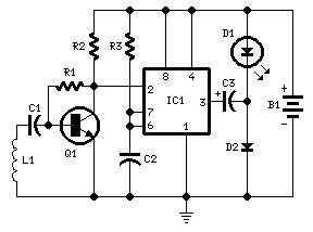
Parts:
R1 100K 1/4W Resistor
R2 3K9 1/4W Resistor
R3 1M 1/4W Resistor
C1,C2 100nF 63V Polyester Capacitors
C3 220µF 25V Electrolytic Capacitor
D1 LED Red 10mm. Ultra-bright (see Notes)
D2 1N5819 40V 1A Schottky-barrier Diode (see Notes)
Q1 BC547 45V 100mA NPN Transistor
IC1 7555 or TS555CN CMos Timer IC
L1 Sensor coil (see Notes)
B1 1.5V Battery (AA or AAA cell etc.)
Device purpose:
This circuit was designed to detect when a call is incoming in a cellular phone (even when the calling tone of the device is switched-off) by means of a flashing LED.
The device must be placed a few centimeters from the cellular phone, so its sensor coil L1 can detect the field emitted by the phone receiver during an incoming call.
Circuit operation:
The signal detected by the sensor coil is amplified by transistor Q1 and drives the monostable input pin of IC1. The IC's output voltage is doubled by C2 & D2 in order to drive the high-efficiency ultra-bright LED at a suitable peak-voltage.
Notes:
Stand-by current drawing is less than 200µA, therefore a power on/off switch is unnecessary.
Sensitivity of this circuit depends on the sensor coil type.
L1 can be made by winding 130 to 150 turns of 0.2 mm. enameled wire on a 5 cm. diameter former (e.g. a can). Remove the coil from the former and wind it with insulating tape, thus obtaining a stand-alone coil.
A commercial 10mH miniature inductor, usually sold in the form of a tiny rectangular plastic box, can be used satisfactorily but with lower sensitivity.
IC1 must be a CMos type: only these devices can safely operate at 1.5V supply or less.
Any Schottky-barrier type diode can be used in place of the 1N5819: the BAT46 type is a very good choice.
author: RED Free Circuit Designs
e-mail:
web site: http://www.redcircuits.com/
2N3055 Power Amplifier
Simple and low cost. The optimal supply voltage is around 50V, but this amp work from 30 to 60V. The maximal input voltage is around 0.8 - 1V. As you can see, in this design the components have a big tolerance, so you can build it almost of the components, which you find at home. The and transistors can be any NPN type power transistor, but do not use Darlington types... The output power is around 60W.
Some comments:
- capacitor C1 regulates the low frequencies (bass), as the capacitance grows, the low frequncies are getting louder.
- capacitor C2 regulates the higher frequencies (treble), as the capacitance grows, the higher frequencies are getting quiter.
- this is a class B amplifier, this means, that a current must flow through the end transistors, even if there is no signal on the input. This current can be regulated with the 500ohm; trimmer resistor. As this current incrases, the sound of the amplifier gets better, but the end transistors are more heating. But if this current decrases, the transistors are not heating so much, but the sound gets worse...
Circuit diagram
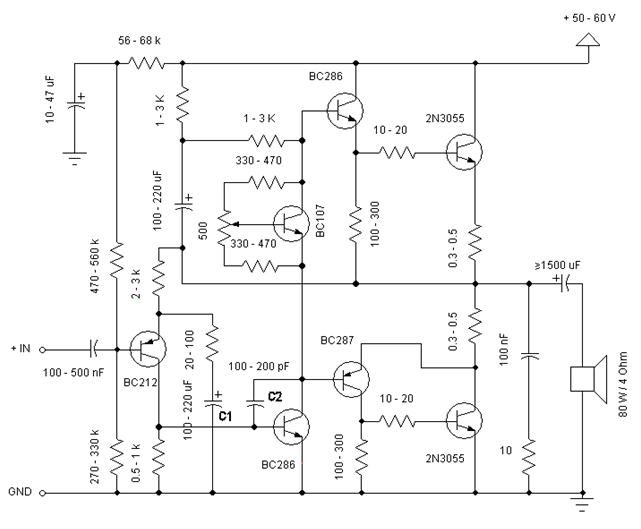
author: Jacint Chapo
e-mail: jacintch@gmail.com
web site: http://www.electronics-lab.com
Simple Radio Receiver with LM386 IC
Listening the programme over the headphones has its advantages, but the true radio receiver is certainly the one that with the loudspeaker. In this project the simplest such receiver is being described, consisting of input circuit, diode detector and audio amplifier with LM386 IC, that allows the loudspeaker reproduction to be performed. 
Click on the image to view circuit
The author has firstly met with the LM386 circuit over twenty years ago, and has ever since been using it very successfully in various devices. The fact that this IC has survived at the market for such a long time is a considerable proof of its quality, however, its most significant advantage remaining extremely low price. The readers can find more information on this circuit in book 4 of PE. Purchasing this IC, one must have in mind that it is being manufactured in several versions, marked as LM386, LM386N-1, LM386N-3 and LM386N-4, that differ themselves by the supply voltage values and the output power. In case the supply voltage being no greater than 12 V, any of these can be used in this receiver.
Electronic diagram of the direct radio receiver that has a LM386 IC in its LF stage is given on Pic.3.18. The resistor in the detection circuit is the log type 470 kOhms potentiometer. The LF voltage is being led over its moving end and the coupling capacitor C2 onto the inverting input (leg No.2) of the LM386. Other, non inverting input (leg No.3) is connected to the ground. The output is on the leg No.5. On this leg the load (i.e. 8 Ohm impedance loudspeaker) is being placed, connected over the C6 capacitor to the ground. With smaller battery power supply voltages a 4 Ohm impedance loudspeaker can also be used. If there's nothing in between the legs 1 and 8, the voltage amplification of the IC is Au=20, in which case the capacitor C7 can be omitted. If, however, a 10 ìF electrolytic capacitor is connected between legs 1 and 8 (+ end on leg 1) as shown on Pic.3.18, the amplification is Au=200. Adding a resistor in line with the abovementioned capacitor, any amount of amplification between 20 and 200 can be achieved. This resistor is shown in dashed line on Pic.3.18 and is being marked with "*" sign.
The PCB and components layout for the receiver shown on Pic.3.18 are given on Pic.3.19. Miniature loudspeakers from the pocket-size radio receivers should be avoided, since their efficiency and sound quality are poor, especially in the low frequencies area. On Pic.3.19 a 1W loudspeaker is being shown, whose membrane is 8 cm in diameter. That isn't such a bad solution, but even better would be using the loudspeaker with greater power and membrane diameter (During the testing the 3 W , 8 Ohm loudspeaker has also been used, and the sound quality was much better than with the one that is shown on the picture). As you can see, the cables connecting the loudspeaker with the PCB are firmly twisted around each other. This is a must, especially for the cables being longer than a dozen centimetres. The same has to be done with cables that connect PCB with the battery and the main switch Z.
Significantly louder reception, with bandwith being narrower in the area of the lower bound frequency, can be accomplished with the coil that has smaller inductivity and the coupling capacitor CA with greater capacitance. For example, if you are interested in radio stations that emits the signal in the MW area from 750 kHz to 1700 kHz, you could use the coil that has been previously described, by using only its' part between the legs 1 and 2, as shown on Pic.3.20. For the antenna that is about 6 m long use the CA=33 pF, and the reception is going to get better. Try increasing the CA capacitance (47 pF, 100 pF, 200 pF), the reception is going to get louder and louder, but the reception bandwidth will be getting smaller and smaller, some stations will not be heard any more, others will start to "mix" etc. it is up to you to find an optimum that suits you best. If using very short antenna, you should omit CA, and connect the antenna directly to the oscillatory circuit (at pt. 1).

3.5. Radio Receiver with Increased Sensitivity Audio Amplifier
If you cannot obtain the signal reception that is loud enough with receiver from the previous project, the sensitivity of the LF part of the device must be increased. The simplest way to manage this is adding a transistor pre-amplifier, as shown on pic.3.21. Please note that all the components except C1, C and L are located on the PCB, which allows you to use the input circuit from pics.3.15 and 3.20. The receiver is supplied from the 4.5 V battery but, if you intend to use an adaptor, the supply voltage can be bigger, its maximum value being from 12 V (for the LM386) till 18 V (for the LM386-4).
The optimal value for R3 resistor (obtaining the greatest amplification, minimal distortion etc.) depends upon the kind of transistor that is being used. The easiest way to finding it is by experimenting, with a few MOhms’ trimmer resistor, in the way it has already been described in chapter 3.2.

3.6. Universal Audio Amplifier
In majority of the receivers described so far, as well as in many those that will be described further, an audio amplifier is being used. This makes it useful to build an universal amplifier that would be used during testing of all receivers. That can be the circuit from pic.3.21 (from C4 inclusive to the right), but it can be something else, too, e.g. the one from the pic.3.22. Two IC’s are used in it: operational amplifier TLO71 as the pre-amplifier, and LM386 as the power amplifier. The TLO741 is exactly the same as the more famous 741, the only difference laying in fact that TLO71 has the FET on its input, and 741 - the bipolar transistor. Since inverting input is being used in the operational amplifier, its voltage amplification is given by Au=RP/R1, where RP stands for the potentiometer resistance from the sliding contact to its left end. When the slider is at its rightmost position, it is then RP=470 kOhms, yielding Au=470, and when it’s at its leftmost position the RP=0, therefore Au=0. As you can see, moving the slider changes the amplification from 0 to 470. That’s what theory says, the practice is, of course, somewhat different. When capacitors are being connected between the input and ground, maximum amplification gets lower than 470 but is still more than enough for our needs.


* All the receivers that have been described so far, as well as all those to come, can be tested with this universal amplifier. That is done by taking the signal from the Detector output (through two wires as short as possible or through the microphone cable that can be significantly longer) to the amplifier input (between left end of C1 and Ground). If the antenna, input circuit (and other stages, if exist) are OK, you will be able to hear the tuned station program from the loudspeaker. The sound volume can be adjusted by moving the slider of the potentiometer P. PCB and component layout are given on pic.3.23.
* KS marks the short-circuit wire. It’s a piece of wire which ends are taken through the holes on the plate and soldered. It can be omitted, but then the left end of potentiometer is to be soldered in such a way to be connected to the bottom end of R1.
* To connect the potentiometer with the PCB, as well as the male, a shielded cable should be used. The shield (outside conductor) is connected to the Ground. If cables are shorter than app. 10 cm, the ordinary wires can be used instead.
* The amplifier, the loudspeaker and the battery (or adapter) are put in the common box, on whose front plate the potentiometer, the switch and some simple plug (the chinch will do) are mounted. If the device is powered from the adapter, it is useful to also mount a LED. With these parts you have made yourself the so-called “active loudspeaker”, which is a very useful gadget for every electronics lover.
* Just before you start mounting and soldering the components, clean well the PCB copper conductors with a piece of wet sponge dipped in some cleaning powder. Components should be mounted and soldered in the following order: short-circuits, resistors, IC’s, capacitors (all except C4), connecting wires and microphone cables (if used). The last component to be mounted is the C4 capacitor, but first you have to check whether the amplifier operates correctly.
Connect the loudspeaker, and the wire marked as “B” on pic.3.23-c connect to the minus battery pole. The other end of the wire marked as “A” should be connected to one probe of the multimeter, which is to be set to measure DC current. Contact the plus battery pole with second instrument probe, and it will measure the idle current of the amplifier, which should be app. 5 mA. If this is OK, touch the pin No.2 of the LM386 with finger, and if everything is fine you will hear the 50 Hz hum from the loudspeaker. The power amplifier is OK. You can now solder C4. Touch the left end of the wire that is connected to the C1 with your finger, the hum should be heard again from the loudspeaker, its loudness depending upon the position of the slider of the potentiometer P. (If you don’t possess an instrument, connect the battery on the wires “A” and “B” and do the touching described. If you hear the hum, the amplifier is OK).
If the Idle current is zero or is significantly bigger than 5 mA, something is wrong. If it’s zero, check out whether you have connected your instrument properly and whether it is functioning. Remove the instrument and connect the battery directly to the wires A and B. Touch the pin No.2 of LM386 with your finger, if you hear the hum - your instrument is malfunctioning. However, if the instrument is OK, you should check the DC voltages. Set your multimeter to measure DC voltages, connect one probe (the one marked with the ground sign) to the amplifier ground (minus battery pole) and with second probe touch the plus battery pole first, and then pin No.6 of LM386. These two voltages should be equal to the battery (supply) voltage. Contact then pin No.7 of the TLO71. This voltage should be slightly smaller than the supply voltage. Voltages at pin No.5 of LM386 and No.7 of the TLO71 should be app. equal to the one half of the supply (battery) voltage.
Try to locate the malfunction based on your measurements. Check out if there are some discontinued copper lines on the print, or if two adjacent lines are connected (by themselves or by a small piece of tin that you dropped from the iron during soldering), whether all junctions are the way they should be, if you happened to mount some electrolytic capacitors or IC’s upside-down, etc.
When you make sure that everything is fine, un-solder the potentiometer and the loudspeaker and put them on the front box panel. Also mount the plug and the switch, the LED (if used) etc. Tighten the plate with two small wood screws to the side pane, placing the LM386 on top (above the TLO71). Two distant-rings are to be mounted between the plate and the wood, making the distance between them a few (say, 5) mm. (These rings can be cut from some small plastic pipe). The screws are first to be put through the plate holes, then the rings and then screwed in the panel. After all this you can connect the loudspeaker, the switch, the battery, etc.
AM Radio Receiver Using the NE602 Balanced Mixer Pictured above is a little AM superhetrodyne receiver that covers the broadcast band from 550 Khz
AM Radio Receiver Using the NE602 Balanced Mixer


Pictured above is a little AM superhetrodyne receiver that covers the
broadcast band from 550 Khz to 1650 Khz. The  circuit employs the 8 pin
Signetics balanced mixer IC (NE602) which converts the incoming RF signal
to the standard 455 Khz IF signal and provides about 13dB gain. The IF
signal is amplified by a single transistor stage and audio is recovered
using a biased shotkey diode (5082) and JFET buffer transistor. The LM386
audio amp is used to drive a small 2.5 inch speaker at about 200 milliwatts.

The circuit contains four LC tuned circuits, all of which need to be fine
tuned to obtain good results. An oscilloscope and RF signal generator are
useful, but the circuit can also be setup using local radio stations
and an additional portable AM radio.

For test purposes, the circuit can be assembled on a solderless breadboard
so changes can easily be made. Try to use short connections for the RF
section with the antenna loop a couple inches away from the board.

Assemble the NE602, ferrite antenna loopstick, tuning cap, oscillator coil
and associated other parts on the breadboard.

Next, connect the battery through a DMM and verify 3 or 4 milliamps of
current flow.

Next, adjust the tuning cap for maximum capacitance (550KHz) and connect
a scope to pin 6 of the NE602 and verify a approx 1 volt p-p sine waveform.
Adjust the red slug of the T1 oscillator coil for a frequency of about
1 MHz. Then adjust the capacitor to minimum capacitance and verify the
frequency increases to around 2Mhz.

To adjust the oscillator without a scope, use a portable AM radio to
verify the oscillator is working and the frequency is right. To do this,
place the portable radio close to the antenna coil and tune it to a AM
station around 1000 on the band. Set the circuit tuning dial to the station
frequency minus 455KHz. For example, if the portable radio is set to 1100,
the circuit tuning dial should point to (1100-455 = 645KHz). This doesn't
have to be exact, but set things as close as you can. Next, adjust the red
oscillator coil slug until a beat frequency is heard on the portable radio.
You should hear a squeal and then a null as the oscillator frequency gets
near the station point on the band. This will verify the oscillator is
running at about 455 Khz above the dial setting.

If the oscillator doesn't run, the problem may be the connections to the
(red) oscillator coil. The red oscillator coil will have 5 connections,
3 on one side for the tapped primary, and 2 on the other for the secondary.
The circuit requires only the single, tapped primary side, but unfortunately
the primary tap is too close to one end for the circuit to operate. To
overcome this problem, the secondary is added in series with the primary
which effectively moves the tap closer to the center and provides more
feedback to sustain oscillations. The phasing of the secondary connections
is also important. If the oscillator fails to work, try reversing the
connections to the secondary of the coil. When the oscillator is setup,
the remainder of the receiver can be assembled and calibrated.

If you have a signal generator, set it for 600KHz, 30% audio modulation
and 1 volt output. Connect the generator through a 1K resistor and a couple
turns of wire around the antenna loopstick. Adjust the yellow and black coil
slugs and also the position of the antenna coil on the loopstick for
strongest response. Reduce the generator output as the signal improves so
you can find a peak for all three coils. You can also make small adjustments
to the oscillator coil to get the tuning dial to point directly at 600.
This will calibrate the low end of the band. To calibrate the high end,
set the generator for some frequency near the high end, maybe 1500 on the
dial. Tune the receiver so it receives the signal and then adjust the two
trimmer capacitors located on the back of the tuning capacitor for best
response. You may find at this point the trimmer caps are all the way
closed or open and a peak cannot be found. To fix this problem, note which
way the caps are set and slightly adjust the main tuning dial to compensate.
For example, if the caps are all the way closed, move the tuning dial to a
lower setting (more capacitance) and then repeak the trimmers. Continue this
until you can find a peak where the trimmers caps are not fully closed or
open. At this point, repeat the adjustments at the low and high end until
both are optimum.

This same procedure can be done without the generator using a couple local
radio stations at opposite ends of the band. The first thing to do is
identify a station that can be heard somewhere on the band. Try to do this
without adding an external antenna, but if no stations are heard, add a short
2 foot wire antenna to the antenna input at the gate of the JFET. Find the
strongest station and slide the antenna coil along the loopstick for best
response and also adjust the yellow and black IF coils. Here is a step by
step procudure I found works reasonably well. My test station was located
at 790 on the band.

1. If no stations are heard, connect a short 2 foot wire antenna to the
  junction of the antenna loopstick and gate of the JFET.

2. Adjust the tuning capacitor and slide the antenna coil for best response
  of some local station.

3. Adjust the yellow and black slugs of T2 and T3 for loudest response.

4. Reduce the length of the wire antenna and readjust the position of the
  antenna coil for best response.

5. Move the tuning dial slightly toward the correct point without losing the
  station. (i.e.) If the station is located at 700 and your tuning dial is
  pointing higher at 750, slightly move it down toward the correct 700 point
  (more capacitance).

6. Readjust T2,T3 and antenna coil for best response.

7. Repeat steps 4, 5 and 6 until the station is heard loud and clear and
  no further improvement can be made.

8. Remove the wire antenna and readjust the antenna coil, T2 and T3 for best
  response. Note the antenna coil should not end up at the center of the
  loopstick. This will indicate not enough inductance and a few more turns
  of wire may be needed on the antenna coil. The optimum position for the
  coil is near the center, slightly offset toward one end. If it ends up very
  near one end of the stick, you may want to remove a few turns which will
  allow the coil to be closer to the center.

9. At this point, several stations should be heard loud and clear but
  minor adjustments may be needed to optimize the entire band. Select
  a station near the bottom of the band (600KHz) and adjust the
  antenna coil and oscillator coil for best response. Note that only
  very small adjustments to the red oscillator coil may be needed.
  Then select a station near the top of the band (1500Khz) and adjust
  the 2 trimmer caps on the back of the main tuning capacitor for best
  response. Repeat this process until both ends are optimized. Be sure
  the 2 trimmer caps do not end up fully open or closed. If they do,
  note the position and slightly adjust the main capacitor to compensate.
  For example, if the trimmers are fully closed, adjust the main capacitor
  slightly lower (more capacitance) and then readjust the trimmers
  so the peak occurs somewhere between min and max.
AM Radio Receiver With Additional IF Stage


Pictured above is the same circuit with an additional IF stage added for
greater sensitivity. Overall gain can be adjusted with the 1K resistors
in the emitter leg of the 2N3904 transistors. The circuit board was assembled
using multiturn 10K pots in place of the 1K resistors and then adjusted for
best performance. The pots are the 2 little blue items just to the left of
the tuning cap. I think I ended up with about 750 ohms. The emitter bypass
caps are not needed since there is plenty of gain available without them.
The caps (two yellow items near the pots) are still in the board but not
connected. I didn't know if they were needed or not, so I put them in there
anyway and later disconnected them. Removing the bypass caps also increases
the input impedance so that both IF stages can use the black IF coils which
have higher secondary impedances (and thus more voltage) than the yellow or
white coils. You might be able to replace the yellow coil with a black one
for greater signal transfer since the input to the first transistor is much
higher without the bypass cap, but I didn't try it. You may notice one of the
black coils is actually white in the picture but it was rewound for a higher
secondary impedance. Actually, it was removed from a junk radio purchased for
a dollar and didn't have any secondary, so I added a 27 turn secondary which
is close to what the black coils use. Overall, the performance is very good
except for the AGC circuit, which has limited range and may not be able
to compensate for very strong stations which may overload the circuit.
The AGC voltage is derived from the IF amplitude at the cathode of the
detector diode (output of T4). As the IF amplitude increases, the DC
voltage at the gate of the JFET will move negative, below ground.
The audio signal is present on both the gate and source terminals of the
JFET, but the audio DC offset voltage will change as the IF amplitude
changes. This DC voltage (about 2 volts) is fed back through a 15K resistor
and the two IF coil secondaries to control the transistor bias points.
The audio signal is filtered out by the 47uF cap leaving a stable DC
voltage at the base of the transistors. As the base voltage drops, the
emitter voltages also drop resulting in less operating current and lower
gain for two IF stages. But the range is limited to maybe only 6-12dB
which isn't enough to compensate for very strong signals. One solution
to the problem is a manual gain control consisting of a switch and
a few turns of wire around the antenna coil which can be seen in the
picture (3 turns of solid insulated white wire on left side of loopstick).
Closing the switch loads the antenna coil and reduces the signal level.

Notes:

IF transformer data and Mouser part numbers can be found at:

http://www.electronics-tutorials.com/filters/if-amplifier-transformers.htm

There are a couple different versions of the yellow and black transformers.
The total turns used and position of the tap varies with the version.
I'm not sure which is better, or which ones I used since they were recovered
from old radios. However, either version should be driven using the
shortest section of the primary. This means connecting the transistor
collector to either the tap or the end closest to the tap and the power
connection to the other point. Leave the transformer end farthest from the
tap unconnected. You can use a DMM to measure the resistance from the tap to
each end of the primary to determine which end is closest to the tap.
Resistance will probably be a couple ohms or less.

A couple sources for ferrite rods for antenna loopsticks can be found at the
links below but the longer rods are expensive ($25 for a 5.6 inch rod).
The second source has 7.5 inch rods for $20. You may also find them on ebay.

http://www.stormwise.com/page26.htm
http://www.universal-radio.com/catalog/misc/amidon.html

A source for a miniture variable tuning capacitor was found at
"Ocean State Electronics" http://www.oselectronics.com/ose_p98.htm

Near the bottom of the page is the listing:

Miniature 2 Gang Poly-film Variable Tuning Capacitor For Broadcast Band

" Tunes AM band from 540Khz to 1600Khz. Ideal variable tuning capacitor
for miniature circuitry and use as exact-duplicate replacement in current
transistor receivers. Rotates through a full 180 degrees
Maximum capacity: Antenna section. 15-140PF, Oscillator section, 10-60PF.
Trimmer capacity: variable to over 12PF. Trimmer adjustment on rear of case.
Completely enclosed to clear polyethylene plastic case to protect plates.
Includes calibrated dial, screw, and knob.
Small size, 3/4" Square x 1/2" Deep.

BC-540...........$3.95 "

If you use this cap or similar from an old miniture radio, the antenna
loopstick inductance will need to be about 600uH to tune 550KHz with the
capacitance at maximum (140pF). This amounts to about 80 turns on a 4 inch,
3/8 diameter ferrite rod. Shorter rods will need more turns.
Loop Antenna for AM Radio


A loop antenna can greatly improve medium wave reception. Loop antennas
are directional and receive signals along the plane of the windings. The
directional quality improves signal to noise ratio of the desired signal
while rejecting signals perpendular to the plane of the windings. Larger
loops are better than smaller ones but good results can be obtained
from moderate sizes of one or two feet on a side. The shape doesn't
make much difference so the loop can be circular, rectangular or
a triangle shape. The main idea is to cover as much area as possible,
so I would imagine a circular loop would be the best. The loop pictured
here measures 15 inches on a side and is about 1.5 inches wide. It was
wound with 16 turns of #35 copper wire, and has a Q of about 100 at
600 KHz. Larger guage wire might have been better (less resistance)
and therefore higher Q and selectivity, but the arrangment here works
pretty well with a bandwidth of about 6Khz at 600Khz. The loop is tuned
with a 30-365 pF capacitor and covers the standard broadcast band of
550-1700 KHz. The antenna signal is inductively coupled to the radio's
internal ferrite rod antenna so no wire connections are needed.
Simply place the radio near the loop antenna and adjust the position(s)
for best results. You may have to adjust the tuning of both the radio
and antenna several times for optimum results.


More detailed information on loop antennas can be found at:
 AM Loop Antennas

A calculator for figuring the number of turns needed for various
rectangular loops can be found here:

Loop Loop Antenna Calculator - By Bruce Carter
Miniature Receiver with ZN414 (ZN414Z) IC
The receiver from Pic.3.25 can be made portable (without an external antenna) if ferrite antenna is used instead of the carton-body coil, right? Well, not exactly. The ferrite antenna is a directional - type antenna, meaning that it does matter where are the waves made by transmitter coming from. The voltage being induced in it under the effect of EM field is the biggest if the ferrite rod is in horizontal position, aimed in such a manner that its axis is perpendicular to the direction of spread of the waves (i.e. perpendicular to the direction towards the transmitter). If the rod is being turned (in horizontal plane), the voltage decreases and gets to minimum when the rod is turned for 90 degrees, i.e. When the rod axis is parallel to the direction pointing towards the transmitter. That means that when the receiver from Pic.3.25 (with the ferrite antenna) is tuned to some station, the reception can be additionally improved by simply rotating it. The directional feature of the antenna is useful here. This, however, can be bad if the receiver is used in motion, since the volume would be constantly changing, and the receiver should be constantly turned towards the transmitter. It would clearly prove itself useful to have an electronic circuit in the receiver that would be automatically changing the amplification of the receiver, in such a manner that it would be increased when the signal in the antenna weakens and vice versa. This would even be convenient in the stationary - type receivers, since it would provide the constant sound strength in the loudspeaker during the reception of signals of various power. Such circuit does exist in modern receivers, and is called the Automatic Amplification Regulation circuit (AAR).
AAR circuit could be added to some of the receivers described in previous projects. The mishap is that electrical diagrams would then become significantly more complex, which would reflect itself both on the price and the realizability. The solution, however, does exist, and is rather simple: it’s the ZN414 IC, being promoted as an “AM Receiver”. Its block diagram is given on the Pic.3.30. The signal from the input


circuit (with ferrite antenna) is led on pin 2 of the IC, which is the input of the amplifier (Z) that has very big input impedance (about 4 MOhms). This is very significant, since such amplifier does not load the oscillatory circuit and doesn’t reduce its Q- factor. The signal is then being amplified through 3-stage HF amplifier (HFA) and demodulated in the detector, thereby exiting the IC as an LF signal (music, speech...). In the right part of the Pic.3.30 the pin description of the ZN414 is given. As you can see, it is placed in a housing usually used for small-power transistors, either plastic (on top, like BC547) or metal (bottom, like BC107).
One end of the oscillatory circuit is connected to the ground over the C1 capacitor (for AC voltages), since input into the amplifier Z is between pin 2 and the ground, where the input signal is to be brought.
The automatic amplification regulation (control) is achieved by returning the DC component of the detected signal from the output to the input of the IC, over the R1 resistor. This DC voltage is being created on R2 resistor. It is substantial for the correct operation of ZN414, its resistance must be such that DC voltage on the pin 1 (to the ground) when no station is being received, is equal to 0.9 V. While calculating the R2 one must have in mind that the idle current of the IC goes through it, its typical value being 0.3 mA, and maximum 0.5 mA (more data about ZN414 can be found in table on Pic.3.36).
The electrical diagram of a small portable MW radio receiver, reproduction being done over the headphones, is given on Pic.3.31. The LF signal is led from the ZN414 output over the coupling capacitor C3 to simple amplifier made with BC547 transistor (or similar), which we discussed about before. This can even be done without the LF amplifier. If you have high-resistance headphones that are sensitive enough connect them between the right end of C3 and the ground, and omit the transistor, R3 R4 and C4.
The 1.5V battery is being used in this device, therefore the necessary 0.6V voltage drop is done with R2=1.5 kOhms. You should, just in case, connect first a 5 kOhms trimmer instead of R2, put its slider in the mid position, turn on the receiver and set it on an empty place on the scale, where no signal can be heard. Connect the voltmeter between the pin1 and ground, and carefully move the slider until the instrument shows 0.9V. If you have no instrument, tune the receiver to some station and move the slider carefully until you reach an optimum receipt. Then turn the variable capacitor’s knob across the entire scale, to ensure that receiver is working well throughout the entire reception range. If everything is OK turn off the receiver, disconnect the trimmer, measure its resistance and solder an appropriate resistor on the PCB. While experimenting with R2 please have in mind that its resistance should be in any case no less than 600 Ohms.
On Pic.3.32 the PCB, ferrite antenna and look of entire device are shown.
If you plan to make a different PCB, since the device works on high frequencies, you have to obey certain rules in order to have a reliable and stable operation:
a. The splitting capacitor C2 has to be mounted as close as possible to the pin 1 of the ZN414. Its capacitance affects both the amplification (which increases with increase of C2) and the limit frequency of the LF signal (which decreases with increase of C2), so the compromise has to be found. You may put for start C2=82 nF (or even 100 nF), and if the reproduction quality pleases you - everything is in order. You could try with smaller capacitance, the amplification will decrease but the reproduction will be better, etc.
b. All the connections, especially those near the ZN414, must be kept as short as possible.
c. The ferrite antenna and variable capacitor should be placed as far away from the battery, loudspeaker (if existing) and the cables connecting them to the PCB.
d. The rotor (G- leg) of the variable capacitor must be connected with the junction of R1 and C1.
Regarding the ferrite antenna, the best thing would be using some that is retrieved from some disused conventional receiver, more on this was told in the project No.3.8. If you can’t find one, or it is unsuitable for some reason, you can make it according to Pic.3.32-c. The length of the ferrite rod is 42 mm. If you have a longer rod, cut it down to size. This cannot be done with the saw, but a groove must be made with the rasp all around, after which the rod can be simply broken in two. The coil body is, again, made of paper tape that is spooled and glued onto the rod. Before you start with spooling, several pieces of 0.5 mm wire (3 on the picture) should be inserted between the rod and the paper. The coil has got 80 quirks of lacquer -isolated copper wire, its diameter being app. 0.2 mm. The beginning and the end of the coil are fixed with the scotch tape (the starting quirks are pressed on the coil body and fixed with several reels of 3 mm tape. The same is done with the ending ones). When the body is finished, the wires are removed. It is thus achieved that the coil body doesn’t lay firmly on the rod, which can now be moved side-to-side, changing thereby the inductance of the coil, so that its optimum value can be established. If you still decide not to use the ferrite antenna, you can use our coil from Pic.3.6. In that case, the leg should be kept “in air”, i.e. it is not used.

* The battery can be connected to the PCB with two pieces of wire that are soldered to it. This solution is fine if you are skilled in soldering and can easily un-solder the old battery and attach the new one. But if you intend to give the receiver to someone, and he/she is not a soldering-lover, you’ll have to find another solution. The simplest thing to do is take the battery housing from an old receiver, do the necessary adjustments and connect it with the PCB with two pieces of flexible (litz) wire. If you cannot do the former, make two battery platforms of brass, as shown on Pic.3.33 and solder them on two copper areas on PCB that are big enough to support them. If you accept this solution, your PCB must be bigger (The additional part is shown in dashed line, on Pic.3.32-a). The board now also contains the holes for the screws, which are fixing it onto the device box. On the platform that supports negative (-) battery pole, a small spring can be attached, to provide a good contact. If you don’t have such a spring, bend the platforms inwards a little, to keep the battery firmly in place.
If you are using a power source whose voltage is greater than 1.5 V, the R2 resistance should be increased. The exact value for it is best to find as previously described, by using the 50 kOhms trimmer. Even better solution is using one of the circuits from the Pic.3.34. Which one should it be? The one on the Pic.3.34-d gives the best operating performance. The setting is done with the TP trimmer. The slider is put in the lowest position, and then is slowly moved upwards until the voltage on the pin 1 doesn’t reach the level required. However, this circuit applies a big load onto the battery, surging from it the current I=(9V-3V)/680Ohm=8.8 mA.


3.11. Pocket Receiver with ZN414 & LM386 IC’s
The author was taking notes in his lab while testing the receivers being described herein, and used them later to write this book. One remark about the receiver whose electrical diagram is given on Pic.3.35 was: “Works EXCELLENT”. The reader will probably ask himself: Isn’t this the aforementioned “The Best Receiver”? No, it isn’t, just remember: DE GUSTIBUS... If, however, you consider it to be “The One”, please send your vote on E-mail: tesla@drenik.net;
This device is very similar to the one being described in the previous project. The most important difference is that the LF signal exiting the ZN414 does not go to the transistor amplifier but to the power amplifier built around the LM386, which was used in some previous projects. Any other audio amplifier can be used instead, e.g. those on Pics. 3.15, 3.21 and 3.22.
With this receiver, special care should be taken regarding the voltage on pin No.1. As you did in previous project, put the potentiometer’s slider in mid-position, turn the receiver on and tune it to some station. Move the slider carefully, until you reach the optimum reception. Start changing the capacitance of the variable capacitor, covering its entire scope, to make sure that receiver works well in its entire operating range. If a problem occurs, re-position the slider again. When everything gets OK, turn the receiver off, disconnect the potentiometer, measure its resistance, and solder the resistor of such resistance on the board. The R2 resistance must be no less than 600 Ohms.

from: http://www.mikroe.com/old/books/rrbook/chapter3/chapter3g.htm
Subscribe to:
Posts (Atom)