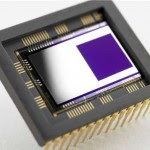
 Charge Coupled Device
![]() CMOS Active Pixel Sensor
CMOS Active Pixel Sensor
Since posts on Charge Coupled Device and CMOS Active Pixel Sensor have already been posted, it is time to know their comparison, advantages and disadvantages. Though both of them are equally used in cameras, there are some differences in parameters like gain, speed and so on.
Comparison – Charge Coupled Device and CMOS Active Pixel Sensor
- Both the devices are used to convert light into electric signals and are used for the same applications. After converting the signals, they have to be read from each cell. This process is different for both the devices.
- The charge from each chip is taken to the end of the array and then read in a CCD. This is then converted into a digital signal with the help of an analog to digital converter (ADC). The process of reading the signal by CMOS Active Pixel Sensor is done by using transistors and amplifiers at each pixel and then the signal is moved using traditional wires.
Difference – Charge Coupled Device and CMOS Active Pixel Sensor
- CCD image sensors create super quality pictures. They also produce lesser noise than CMOS APS.
- In a CMOS all the transistors are kept right next to each pixel. As a result, all the photons that hit the device actually get scattered by hitting the transistors as well. Thus, the sensitivity of CMOS Active Pixel Sensor is lesser than that of a Charge Coupled Device.
- The design of the CCD sensors is in such a way that they require more power for its operation. If both the devices of equal reception are taken, the CCD is considered to consume almost 100 times more power than its equivalent CMOS Active Pixel Sensor.
- All the devices have been using Charge Coupled Device devices far more than CMOS Active Pixel Sensor. As a result a vast study has been done on CCD devices. So, they are more mature and also tend to have higher quality pixels.

EmoticonEmoticon