Simple Transistor Amplifier(LOW POWER)

A very simple low power three stage transistor amplifier circuit is shown below. First and second stages are pre amplifiers and third is the output stage. Collector to base biasing is employed for each stages and it is enough for circuits like this.

Collector to base biasing: Consider the first stage.R1 is the collector resistor and R2 is the base resistor. This type of biasing provides some negative feedback, avoids thermal runaway and stabilizes the operating point. When the temperature increases the collector current also increases. This increases the voltage drop across the collector resistance R1 and this decreases the voltage drop across base resistor R2. As a result, base current drops which in turn drops the collector current and thermal runaway is avoided. Stabilization of operating point is achieved by the prevention of variation in collector current with temperature.

When a transistor amplifier is operating, the collector voltage will be phase opposite to the input signal. Since base resistor R2 is connected between collector and base, some fraction of the phase opposite collector voltage is fed back to the input (base) through the base resistor R2 and thus negative feedback is achieved. Negative feed back reduces the voltage gain of the amplifier but it improves the stability.

In the circuit collector of Q1 is coupled to the base of Q2 using the capacitor C2. R3 is the biasing resistor for Q2 and R4 is its collector resistor.Collector of Q2 is coupled to the base of Q3 using the capacitor C3. R5 is the biasing resistor for Q3 and speaker is connected as the collector load. Capacitors C4 and C5 are filters. C1 is the input DC decoupling capacitor.

Simple Transistor Amplifier(LOW POWER)

NOTES:

  • The circuit can be assembled on vero or perf board.
  • Use 9V DC for powering the circuit. A 9V PP3 battery is fine.
  • All electrolytic capacitors must be rated 10 or 15V.
  • An optional protection diode can be added in series to the positive supply line. This protects the circuit from accidental polarity reversals.
  • Type number of the transistors are not very critical. Replacement will not affect the performance to a great extend.
  • Powering the circuit using a mains adapter will induce some noise.
  • Speaker impedance can be 64 ohms or more.
S:circuitstoday.com

Headphone Amplifier(Class A)

Headphone Amplifier(Class A)

Description.

This is the circuit diagram of a Headphone amplifier operating in the class A push pull mode. In class A mode the output device (transistors) conduct over the entire input signal cycle. The maximum possible efficiency for Class A operation is 50% and it further reduces when capacitive coupling is used. But the advantages of Class AB amplifier are no cross over distortion, high fidelity and low harmonic distortion. These amplifiers are most suitable for low power applications.

In the circuit transistor Q1 works as the preamplifier. Resistors R6 and R7 provides potential divider biasing for Q1. Audio input is coupled to the base od Q1 through capacitor C2, resistor R9 and POT R10. Emitter of Q1 is coupled to the base of Q2 through resistor R3. Diodes D1 and D2 provides bias voltage for Q2. Base of Q3 is directly coupled to the collector of Q1. Resistor R5 limits the collector current of Q2 and Q3. C4 and C5 are power supply filter capacitors. Output of the amplifier is coupled to the head phone using the capacitor C3.

NOTES:

  • The circuit can be assembled on a vero/perf board.
  • Power supply can be anything between 6 to 24V DC.
  • I used 12V DC for powering the circuit.
  • Z1 can be a 100 ohms or higher head phone.
  • Electrolytic capacitors voltage rating must be according to the supply voltage you use.

A simple intercom circuit designed based on transistors

A simple intercom circuit designed based on transistors

Intercom circuit with ringer

Description.
A simple intercom circuit designed based on transistors is shown here. This intercom circuit does not require a changeover switch and you can use it just like a telephone and a ringer circuit is also included.
IC1 UM66 and transistor Q1 forms the ringer section. When pushbutton switch S1 is pressed UM66 produces a musical tone. This tone is amplified by Q1 and is coupled to the collector of Q2. Condenser Mic M1 is used to pick the conversation and Q2 is used to amplify it. R2 powers the condenser Mic while C2 is the DC decoupling capacitor for the amplifier stage based on Q2. The next stage of the circuit is a transformer coupled push pull amplifier stage based on L1, Q3 and Q4. Capacitor C5 is the power supply filter while capacitor C4 couples the output of the push pull amplifier to the ear piece.

Connection Diagram:

A simple intercom circuit designed based on transistors

NOTES:

  • Assemble the circuit on a vero board.
  • Use 9V PP3 battery for powering the circuit.
  • The earpiece can be a telephone ear piece.
  • L1 can be a 6V audio driver transformer.
  • S1 is a pushbutton switch while S2 is a ON/OFF switch.
  • Make two identical circuits as per the circui diagram and arrange them as shown in the connection diagram.
S:circuitstoday.com

A complete guide about multi channel surround sound systems and its formats

Multi-channel audio:

Multi-channel audio systems are widely used in modern sound devices. The term “multi-channel audio” means that, the audio system can be capable of handling multiple audio channels (usually called audio tracks) to rebuild the sound on a multi-speaker setup.

Usually two digits separated by a decimal (.) point (2.1, 4.1, 5.1, 6.1, 7.1, etc.) are used to classify the various kinds of speaker set-up, this number basically depending on how many audio tracks are used. Some audio systems only have a single channel (called monophonic sound or single channel audio) or two channels (stereophonic sound or 2.0 channel sound)

The first digit shows the number of primary channels (called satellite units), each of which are reproduced on a single speaker (these speakers are capable for handling the frequency range from 100Hz to 22Khz), while the second (decimal digit) refers to the presence of LFE (Low Frequency Effect), which is reproduced on a subwoofer.

A complete guide about multi channel surround sound systems and its formats

Surround Sound System
Surround sound is a term used to describe a type of audio output in which the sound appears to “surround the listener” by 360 degrees – that is, the technology gives the impression that sounds are coming from all possible directions.

Surround sound is a way to provide a more realistic and engaging experience. All technical aspects aside, surround sound works because multiple audio channels are received through speakers that are positioned at various locations in the room. This is programmed into the source and the sound tracks are decoded when the source is played.

The Surround Sound Setup

The main component of a surround sound setup is a multi channel or digital coaxial/optical audio decoder. Using a DVD/HVD movie, the audio is encoded when the DVD/HVD is produced by packing multiple audio channels into a compressed format for storage. When you play the DVD movie, your DVD player or A/V receiver (commonly called a home theatre receiver) decodes the encoding scheme (i.e. Dolby Pro Logic II or DTS for example). Decoding capabilities of an A/V receiver are built in. Most A/V receivers today can decode Dolby Digital and Digital Theater Sound (DTS) (DTS channel usually a coaxial or optical audio channel. It is a single channel digital pin that multiplexed with several channel. The decoder decodes the DTS sound from single channel to multiple channels), while higher-end receivers may also include DTS-ES or THX Surround.

Multi-channel Surround Sound Systems

  • 5.1 Surround Sound Systems

5.1 Surround sound systems are one of the widely used surround sound setup in home theater systems. Usually- Dolby Digital and DTS encoded in a DVD are 5.1 channel audio formats. 5.1 surround sound technologies produces five channels of sound in the left, right, center, left-surround and right-surround positions. These five channels are the minimum required to produce 5.1 surround sounds. The dot decimal (.1) represents the channel for LFE (low frequency effects), which is usually sent to a subwoofer. Other 5 units are capable for handling the frequency range except low frequency(Usually they are capable of handling the frequency range from 100Hz to 22Khz and no need for any other higher frequency component like tweeter). These five units are usually called satellite units. The arrangements of a 5.1 surround sound setup shown in the picture below.

A complete guide about multi channel surround sound systems and its formats

6.1 multichannel sound technologies is the advanced version of 5.1 surround sound technology. 6.1 technology uses the same set-up as a 5.1 system, but it has the addition of a sixth speaker that takes the rear-center surround position (or back surround position) to provide a more 3-D realistic surround sound effect. 6.1 surround sound uses extended surround sound formats, such as THX Surround EX, Dolby digital ES and DTS-ES. The 6.1 channel surround sound setup is shown in the picture.

A complete guide about multi channel surround sound systems and its formats

7.1 channel audio systems is the modified version of 6.1 channel and also provide more realistic experience than 6.1 setup. In this system splits the single rear-center speaker into individual left- and right-rear surround. These systems are not a true discrete 7.1 channel system as 7.1 formats don’t currently exist. In a true discrete 6.1 surround system, the back center surround position is separate from the surround left (SL) and surround right (SR) positions. A 7.1 channel system uses matrixes extended surround where the left-back and right-back (rear-center surround) multichannel are blended together and stored. The structure of a 7.1 setup is given in the Picture below.
A complete guide about multi channel surround sound systems and its formats

10.2 channel surround is the future surround sound technology that Developed by THX corporation, the name itself, 10.2 is an advanced version of 5.1 technology but 10.2 is twice as good as 5.1. In a 10.2 surround sound 14 channels are used. This includes five front speakers, five surround channels, two LFE and two heights, plus the addition of a second sub-woofer. This technology is considered as future TRUEHD.The Diagram of a 10.2 TrueHD setup is shown below.

A complete guide about multi channel surround sound systems and its formats

Common Surround Sound Formats

  • Dolby Surround

Dolby surround is the consumer version of Dolby analog film decoding. This technology was introduced in 1982 which is capable of handling stereo and hi-fi audio. This audio format is commonly found in VHS and stereo hi-fi systems. In this surround format, the multichannel audio multiplexed into two audio channels (left and right channels)and decoded by using Dolby pro logic decoder ,then it recreates the four channel Dolby surround experience.

  • Dolby Digital

Dolby digital is the standard surround sound format which provides high quality and highly realistic experience. This audio is developed by Dolby Corporation. Dolby digital audio is also known as Audio Codec-3(AC3). This audio format provides a high quality 5.1 surround experience. Normally this audio format used for the creation of DVD and Blue ray movies. Some video games and play station units are also available in this surround sound format.

  • Dolby Digital EX

Dolby Digital EX is the modified version of Dolby digital audio. This extended format contains an additional surround sound unit (called center surround channel) for creation of more realistic experience. Dolby digital EX needs Dolby EX decoder. This surround effect also support 5.1, 6.1, 7.1 channel playback. This audio format usually available on DVD, HVD, blue ray, play stations, DTV broadcasts, etc .

  • Dolby Pro Logic IIx

Dolby Pro Logic IIx is an advanced version of Dolby Digital EX technology. By using this technology, we can expand the 5.1 channel Dolby surround system into 6.1, 7.1, 10.2 channel surround. The Dolby digital prologic usually use three modes for listening (movie, music and game modes).This surround technology provide more rich and depth surround sound effect than conventional surround sound system. This audio is normally encoded in DVD, HVD, BRD HDTV, play stations, etc.

  • Dolby True HD

Dolby True HD surround sound is an advanced version surround sound that provides incredible High Definition experience to the listener. This surround sound format is also known as next generation surround sound format. Dolby True HD format only support HD based media and this technology provides 100% lossless audio encoding, bit rate up to 18Mbps and support 8.1 or higher channel with 24 bit/96Khz audio. This format also supports HDMI. Normally BRD and HVD are used for encoding this true surround.

  • DTS

DTS is another digital surround format developed by DTS Corporation. It is a Multichannel digital surround format widely used in both consumer and commercial applications. The DTS audio system must have a DTS decoder and optical/coaxial digital decoder for decoding this surround. DTS is normally available in a single channel multiplexed format (2.1 to 11.1 channel surround sounds can be multiplexed into a single optical digital or coaxial output format).DTS format is also available on DVD,HVD and BRD’s.

  • DTS-ES

DTS-ES (digital theater sound –Extended Surround) is an advanced version of normal DTS. This surround system is usually available in 6.1 or higher channels. This provides us with more true digital experience than conventional DTS system. This unit also requires an additional DTS-ES decoder for the creation of a back-surround effect. The system is compatible with all current extended surround formats and an auxiliary surround channel is also provided for other applications.

  • TruSurround-XT

TruSurround XT is the next generation of SRS TruSurround. The main advantage of this surround system is that it’s capable of handling 2.1 channel surround to 10.2 channel surround (support head phone media too).Audio is encoded in multiplexed format. and require DTS true surround decoder. This audio usually encoded in BRD’s and HVD’s

S:circuitstoday.com

A complete basic tutorial for 555 timer IC

Tags
This article covers every basic aspect of 555 Timer IC. You may already know that SE/NE 555 is a Timer IC introduced by Signetics corporation in 1970′s. In this article we cover the following information about 555 Timer IC.

1. Introduction to 555 Timer IC

2. 555 Timer IC Pin Configuration

3. Basics of 555 Timer

4. Block Diagram

5. Working Principle

6. Download Data Sheet

1. Introduction

A complete basic tutorial for 555 timer IC

One of the most versatile linear ICs is the 555 timer which was first introduced in early 1970 by Signetic Corporation giving the name as SE/NE 555 timer. This IC is a monolithic timing circuit that can produce accurate and highly stable time delays or oscillation. Like other commonly used op-amps, this IC is also very much reliable, easy to use and cheaper in cost. It has a variety of applications including monostable and astable multivibrators, dc-dc converters, digital logic probes, waveform generators, analog frequency meters and tachometers, temperature measurement and control devices, voltage regulators etc. The timer basically operates in one of the two modes either as a monostable (one-shot) multivibrator or as an astable (free-running) multivibrator.The SE 555 is designed for the operating temperature range from – 55°C to 125° while the NE 555 operates over a temperature range of 0° to 70°C.

The important features of the 555 timer are :

  • It operates from a wide range of power supplies ranging from + 5 Volts to + 18 Volts supply voltage.
  • Sinking or sourcing 200 mA of load current.
  • The external components should be selected properly so that the timing intervals can be made into several minutes Proper selection of only a few external components allows timing intervals of several minutes along with the frequencies exceeding several hundred kilo hertz.
  • It has a high current output; the output can drive TTL.
  • It has a temperature stability of 50 parts per million (ppm) per degree Celsius change in temperature, or equivalently 0.005 %/ °C.
  • The duty cycle of the timer is adjustable with the maximum power dissipation per package is 600 mW and its trigger and reset inputs are logic compatible.

2. IC Pin Configuration

A complete basic tutorial for 555 timer IC

The 555 Timer IC is available as an 8-pin metal can, an 8-pin mini DIP (dual-in-package) or a 14-pin DIP.

This IC consists of 23 transistors, 2 diodes and 16 resistors. The explanation of terminals coming out of the 555 timer IC is as follows. The pin number used in the following discussion refers to the 8-pin DIP and 8-pin metal can packages.

A complete basic tutorial for 555 timer IC

Pin 1: Grounded Terminal: All the voltages are meas­ured with respect to this terminal.

Pin 2: Trigger Terminal: This pin is an inverting input to a comparator that is responsible for transition of flip-flop from set to reset. The output of the timer depends on the amplitude of the external trigger pulse applied to this pin.

Pin 3: Output Terminal: Output of the timer is avail­able at this pin. There are two ways in which a load can be connected to the output terminal either between pin 3 and ground pin (pin 1) or between pin 3 and supply pin (pin 8). The load connected between pin 3 and ground supply pin is called the normally on load and that connected between pin 3 and ground pin is called the normally off load.

Pin 4: Reset Terminal: To disable or reset the timer a negative pulse is applied to this pin due to which it is referred to as reset terminal. When this pin is not to be used for reset purpose, it should be connected to + VCC to avoid any possibility of false triggering.

Pin 5: Control Voltage Terminal: The function of this terminal is to control the threshold and trigger levels. Thus either the external voltage or a pot connected to this pin determines the pulse width of the output waveform. The external voltage applied to this pin can also be used to modulate the output waveform. When this pin is not used, it should be connected to ground through a 0.01 micro Farad to avoid any noise problem.

Pin 6: Threshold Terminal: This is the non-inverting input terminal of comparator 1, which compares the voltage applied to the terminal with a reference voltage of 2/3 VCC. The amplitude of voltage applied to this terminal is responsible for the set state of flip-flop.

Pin 7 : Discharge Terminal: This pin is connected internally to the collector of transistor and mostly a capacitor is connected between this terminal and ground. It is called discharge terminal because when transistor saturates, capacitor discharges through the transistor. When the transistor is cut-off, the capacitor charges at a rate determined by the external resistor and capacitor.

Pin 8: Supply Terminal: A supply voltage of + 5 V to + 18 V is applied to this terminal with respect to ground (pin 1).

3. 555 Timer Basics

The 555 timer combines a relaxation oscillator, two comparators, an R-S flip-flop, and a discharge capacitor.

R-S Flip-Flop: – A pair of cross-coupled transistors is shown in figure. Each collector drives the opposite base through resistance RB. In such circuit one transistor is saturated while the other is cut-off. For instance, if transistor Q1 is saturated, its collector voltage is almost zero. So there is no base drive for transistor Q2 and it goes into cut-off and its collector voltage approaches + VCC. This high voltage produces enough base current to keep transistor Q1 in saturation.

On the other hand if transistor Q1 is cut-off, its collector voltage, which is approximately equal to + VCC, drives the transistor Q2 into saturation. The low collector voltage (which is approximately to zero) of this transistor then keeps the transistor Q2 in cut-off.Depending on which transistor is saturated, the Q output is either low or high. By adding more components to the circuit, an R-S flip-flop is obtained. R-S flip-flop is a circuit that can set the Q output to high or reset it low. Incidentally, a complementary (opposite) output Q is available from the collector of the other transistor.

Figure shows the schematic symbol for an R-S flip-flop of any design. The circuit latches in either two states. A high S input sets Q to high; a high R input resets Q to low. Output Q remains in a given state until it is triggered into the opposite state.

A complete basic tutorial for 555 timer IC

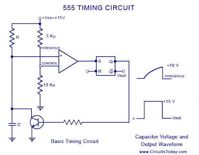
Basic Timing Concept

Figure illustrates some basic ideas that will prove useful in coming blog posts of the 555 timer. Assuming output Q high, the transistor is saturated and the capacitor voltage is clamped at ground i.e. the capacitor C is shorted and cannot charge.

The non-inverting input voltage of the comparator is referred to as the threshold voltage while the inverting input voltage is referred to as the control voltage. With R-S flip flop set, the saturated transistor holds the threshold voltage at zero. The control voltage, however, is fixed at 2/3 VCC (i.e. at 10 V) because of the voltage divider.

Suppose that a high voltage is applied to the R input. This resets the flip-flop R-Output Q goes low and the transistor is cut-off. Capacitor C is now free to charge. As this capacitor C charges, the threshold voltage rises. Eventually, the threshold voltage becomes slightly greater than (+ 10 V). The output of the comparator then goes high, forcing the R S flip-flop to set. The high Q output saturates the transistor, and this quickly discharges the capacitor. The two waveforms are depicted in figure. An exponential rise is across the capacitor C, and a positive going pulse appears at the output Q. Thus capacitor voltage VC is exponential while the output is rectangular, as illustrated in figure.

4. Block Diagram

A complete basic tutorial for 555 timer IC

The block diagram of a 555 timer is shown in the above figure. A 555 timer has two comparators, which are basically 2 op-amps), an R-S flip-flop, two transistors and a resistive network.

  • Resistive network consists of three equal resistors and acts as a voltage divider.
  • Comparator 1 compares threshold voltage with a reference voltage + 2/3 VCC volts.
  • Comparator 2 compares the trigger voltage with a reference voltage + 1/3 VCC volts.

Output of both the comparators is supplied to the flip-flop. Flip-flop assumes its state according to the output of the two compa­rators. One of the two transistors is a discharge transis­tor of which collector is connected to pin 7. This tran­sistor saturates or cuts-off according to the output state of the flip-flop. The saturated transis­tor provides a discharge path to a capacitor con­nected externally. Base of another transistor is connected to a reset terminal. A pulse applied to this terminal resets the whole timer irrespective of any input.

5. Working Principle

Refer Block Diagram of 555 timer IC given above:

Comparator 1 has a threshold input (pin 6) and a control input (pin 5). In most applications, the control input is not used, so that the control voltage equals +2/3 VCC. Output of this comparator is applied to set (S) input of the flip-flop. Whenever the threshold voltage exceeds the control voltage, comparator 1 will set the flip-flop and its output is high. A high output from the flip-flop saturates the discharge transistor and discharge the capacitor connected externally to pin 7. The complementary signal out of the flip-flop goes to pin 3, the output. The output available at pin 3 is low. These conditions will prevail until comparator 2 triggers the flip-flop. Even if the voltage at the threshold input falls below 2/3 VCC, that is comparator 1 cannot cause the flip-flop to change again. It means that the comparator 1 can only force the flip-flop’s output high.

To change the output of flip-flop to low, the voltage at the trigger input must fall below + 1/3 Vcc. When this occurs, comparator 2 triggers the flip-flop, forcing its output low. The low output from the flip-flop turns the discharge transistor off and forces the power amplifier to output a high. These conditions will continue independent of the voltage on the trigger input. Comparator 2 can only cause the flip-flop to output low.

From the above discussion it is concluded that for the having low output from the timer 555, the voltage on the threshold input must exceed the control voltage or + 2/3 VCC. They also turn the discharge transistor on. To force the output from the timer high, the voltage on the trigger input must drop below +1/3 VCC. This also turns the discharge transistor off.

A voltage may be applied to the control input to change the levels at which the switching occurs. When not in use, a 0.01 nano Farad capacitor should be connected between pin 5 and ground to prevent noise coupled onto this pin from causing false triggering.

Connecting the reset (pin 4) to a logic low will place a high on the output of flip-flop. The discharge transistor will go on and the power amplifier will output a low. This condition will continue until reset is taken high. This allows synchronization or resetting of the circuit’s operation. When not in use, reset should be tied to +VCC.

S:circuitstoday.com

a free-running multivibrator(An astable multivibrator) based on 555 timer

An astable multivibrator, often called a free-running multivibrator, is a rectan­gular-wave generating cir­cuit. Unlike the monostable multivibrator, this circuit does not require any ex­ternal trigger to change the state of the output, hence the name free-running. Before going to make the circuit, make sure your 555 IC is working. For that go through the article: How to test a 555 IC for working An astable multivibrator can be produced by adding resistors and a capacitor to the basic timer IC, as illustrated in figure. The timing during which the output is either high or low is determined by the externally connected two resistors and a capacitor. The details of the astable multivibrator circuit are given below.

a free-running multivibrator(An astable multivibrator) based  on 555 timer

Take a look @ 555 Ic Pin configuration and 555 block diagram before reading further.

Pin 1 is grounded; pins 4 and 8 are shorted and then tied to supply +Vcc, output (VOUT is taken form pin 3; pin 2 and 6 are shorted and the connected to ground through capacitor C, pin 7 is connected to supply + VCC through a resistor RA; and between pin 6 and 7 a resistor RB is connected. At pin 5 either a bypass capacitor of 0.01 F is connected or modulation input is applied.


Astable Multivibrator Operation:

For explaining the operation of the timer 555 as an astable multivibrator, necessary internal circuitry with external connections are shown in figure.

a free-running multivibrator(An astable multivibrator) based  on 555 timer

In figure, when Q is low or output VOUT is high, the discharging transistor is cut-­off and the capacitor C begins charging toward VCC through resistances RA and RB. Because of this, the charging time constant is (RA + RB) C. Eventually, the threshold voltage exceeds +2/3 VCC, the comparator 1 has a high output and triggers the flip-flop so that its Q is high and the timer output is low. With Q high, the discharge transistor saturates and pin 7 grounds so that the capacitor C discharges through resistance RB with a discharging time constant RB C. With the discharging of capacitor, trigger voltage at inverting input of comparator 2 decreases. When it drops below 1/3VCC, the output of comparator 2 goes high and this reset the flip-flop so that Q is low and the timer output is high. This proves the auto-transition in output from low to high and then to low as, illustrated in fig ures. Thus the cycle repeats.

Astable Multivibrator using 555 IC -Design method

The time during which the capacitor C charges from 1/3 VCC to 2/3 VCC is equal to the time the output is high and is given as tc or THIGH = 0.693 (RA + RB) C, which is proved below.

Voltage across the capacitor at any instant during charging period is given as,vc=VCC(1-et/RC)

The time taken by the capacitor to charge from 0 to +1/3 VCC

1/3 VCC = VCC (1-et/RC)

The time taken by the capacitor to charge from 0 to +2/3 VCC

or t2 = RC loge 3 = 1.0986 RC

So the time taken by the capacitor to charge from +1/3 VCC to +2/3 VCC

tc = (t2 – t1) = (10986 – 0.405) RC = 0.693 RC

Substituting R = (RA + RB) in above equation we have

THIGH = tc = 0.693 (RA + RB) C

where RA and RB are in ohms and C is in farads.

The time during which the capacitor discharges from +2/3 VCC to +1/3 VCC is equal to

the time the output is low and is given as

td or TL0W = 0.693 RB C where RB is in ohms and C is in farads The above equation is worked out as follows: Voltage across the capacitor at any instant during discharging period is given as

vc = 2/3 VCC e- td/ RBC

Substituting vc = 1/3 VCC and t = td in above equation we have

+1/3 VCC = +2/3 VCC e- td/ RBC

Or td = 0.693 RBC

Overall period of oscillations, T = THIGH + TLOW = 0.693 (RA+ 2RB) C , The frequency of oscillations being the reciprocal of the overall period of oscillations T is given as

f = 1/T = 1.44/ (RA+ 2RB)C

Equation indicates that the frequency of oscillation / is independent of the collector supply voltage +VCC.

Often the term duty cycle is used in conjunction with the astable multivibrator.

The duty cycle, the ratio of the time tc during which the output is high to the total time period T is given as

% duty cycle, D = tc / T * 100 = (RA + RB) / (RA + 2RB) * 100

From the above equation it is obvious that square wave (50 % duty cycle) output can not be obtained unless RA is made zero. However, there is a danger in shorting resistance RA to zero. With RA = 0 ohm, terminal 7 is directly connected to + VCC. During the discharging of capacitor through RB and transistor, an extra current will be supplied to the transistor from VCC through a short between pin 7 and +VCC. It may damage the transistor and hence the timer.

However, a symmetrical square wave can be obtained if a diode is connected across resistor RB, as illustrated in dotted lines in figure. The capacitor C charges through RA and diode D to approximately + 2/3VCC and discharges through resistor RB and terminal 7 (transistor) until the capacitor voltage drops to 1/3 VCC. Then the cycle is repeated. To obtain a square wave output, RA must be a combination of a fixed resistor R and a pot, so that the pot can be adjusted to give the exact square wave.

Although the timer 555 has been used in a wide variety of often unique applications it is very hard on its power supply lines, requiring quite a bit of current, and injecting many noise transients. This noise will often be coupled into adjacent ICs falsely triggering them. The 7555 is a CMOS version of the 555. Its quiescent current requirements are considerably lower than that of 555, and the 7555 does not contaminate the power supply lines. It is pin compatible with the 555. So this CMOS version of the 555 should be the first choice when a 555 timer IC is to be used.

S:circuitstoday.com

One-shot multivibrator (MMV) using 555 timer

A monostable multivibrator (MMV) often called a one-shot multivibrator, is a pulse generator circuit in which the duration of the pulse is determined by the R-C network,connected externally to the 555 timer. In such a vibrator, one state of output is stable while the other is quasi-stable (unstable). For auto-triggering of output from quasi-stable state to stable state energy is stored by an externally connected capaci­tor C to a reference level. The time taken in storage determines the pulse width. The transition of output from stable state to quasi-stable state is accom­plished by external triggering. The schematic of a 555 timer in monostable mode of operation is shown in figure.
One-shot multivibrator (MMV) using 555 timer

Monostable Multivibrator Circuit details

Pin 1 is grounded. Trigger input is applied to pin 2. In quiescent condition of output this input is kept at + VCC. To obtain transition of output from stable state to quasi-stable state, a negative-going pulse of narrow width (a width smaller than expected pulse width of output waveform) and amplitude of greater than + 2/3 VCC is applied to pin 2. Output is taken from pin 3. Pin 4 is usually connected to + VCC to avoid accidental reset. Pin 5 is grounded through a 0.01 u F capacitor to avoid noise problem. Pin 6 (threshold) is shorted to pin 7. A resistor RA is connected between pins 6 and 8. At pins 7 a discharge capacitor is connected while pin 8 is connected to supply VCC.

555 IC Monostable Multivibrator Operation

One-shot multivibrator (MMV) using 555 timer

For explain­ing the operation of timer 555 as a monostable multivibrator, necessary in­ternal circuitry with external connections are shown in figure.

The operation of the circuit is ex­plained below:

Initially, when the output at pin 3 is low i.e. the circuit is in a stable state, the transistor is on and capacitor- C is shorted to ground. When a negative pulse is applied to pin 2, the trigger input falls below +1/3 VCC, the output of comparator goes high which resets the flip-flop and consequently the transistor turns off and the output at pin 3 goes high. This is the transition of the output from stable to quasi-stable state, as shown in figure. As the discharge transistor is cut­off, the capacitor C begins charging toward +VCC through resistance RA with a time constant equal to RAC. When the increasing capacitor voltage becomes slightly greater than +2/3 VCC, the output of comparator 1 goes high, which sets the flip-flop. The transistor goes to saturation, thereby discharging the capacitor C and the output of the timer goes low, as illustrated in figure.

Thus the output returns back to stable state from quasi-stable state.

The output of the Monostable Multivibrator remains low until a trigger pulse is again applied. Then the cycle repeats. Trigger input, output voltage and capacitor voltage waveforms are shown in figure.

Monostable Multivibrator Design Using 555 timer IC

The capacitor C has to charge through resistance RA. The larger the time constant RAC, the longer it takes for the capacitor voltage to reach +2/3VCC.

In other words, the RC time constant controls the width of the output pulse. The time during which the timer output remains high is given as

tp = 1.0986 RAC
where RA is in ohms and C is in farads. The above relation is derived as below. Voltage across the capacitor at any instant during charging period is given as

vc = VCC (1- e-t/RAC)

Substituting vc = 2/3 VCC in above equation we get the time taken by the capacitor to charge from 0 to +2/3VCC.

So +2/3VCC. = VCC. (1 – e-t/RAC) or t – RAC loge 3 = 1.0986 RAC

So pulse width, tP = 1.0986 RAC s 1.1 RAC

The pulse width of the circuit may range from micro-seconds to many seconds. This circuit is widely used in industry for many different timing applications.


S:circuitstoday.com

voltage-controlled oscillator (VCO) using the 555 timer


The circuit is sometimes called a voltage-to-frequency converter because the output frequency can be changed by changing the input voltage.

As discussed in previous blog posts, pin 5 terminal is voltage control terminal and its function is to control the threshold and trigger levels. Normally, the control voltage is ++2/3VCC because of the internal voltage divider. However, an external voltage can be applied to this terminal directly or through a pot, as illustrated in figure, and by adjusting the pot, control voltage can be varied. Voltage across the timing capacitor is depicted in figure, which varies between +Vcontrol and ½ Vcontrol. If control voltage is increased, the capacitor takes a longer to charge and discharge; the frequency, therefore, decreases. Thus the fre­quency can be changed by changing the control volt­age. Incidentally, the control voltage may be made available through a pot, or it may be output of a transistor circuit, op-amp, or some other device.


timer 555 based ramp generator circuit


We know that if a capacitor is charged from a voltage source through a resistor, an exponential waveform is produced while charging of a capaci­tor from a constant current source produces a ramp. This is the idea behind the circuit. The circuit of a ramp generator using timer 555 is shown in figure. Here the resistor of previ­ous circuits is replaced by a PNP transistor that produces a constant charging current.


Charging current produced by PNP constant current source is

iC = Vcc-VE / RE

where VE = R2 / (R1 + R2) * VCC + VBE

When a trigger starts the monostable multivibrator timer 555 as shown in figure, the PNP current source forces a constant charging into the capacitor C. The voltage across the capacitor is, therefore, a ramp as illustrated in the figure. The slope of the ramp is given as

Slope, s = I/C

S:circuitstoday.com

NE555 timer based police siren

NE555 timer based police siren

A lot of electronic circuits using NE555 timer IC are already published here and this is just another one.Here is the circuit diagram of a police siren based on NE55 timer IC. The circuit uses two NE555 timers ICs and each of them are wired as astable multivibrators.The circuit can be powered from anything between 6 to 15V DC and is fairly loud.By connecting an additional power amplifier at the output you can further increase the loudness.

IC1 is wired as a slow astable multivibrator operating at around 20Hz @ 50% duty cycle and IC2 is wired as fast astable multivibrator operating at around 600Hz.The output of first astable mutivibrator is connected to the control voltage input (pin5) of IC2. This makes the output of IC2 modulated by the output frequency of IC1, giving a siren effect. In simple words, the output frequency of IC2 is controlled by the output of IC1.

  • The circuit can be assembled on a Perf board.
  • I used 12V DC for powering the circuit.
  • Instead of using two NE55 timer ICs, you can also use a single NE556 timer.
  • NE556 is nothing but two NE555 ICs in one package.
  • Refer the datasheets of NE555 and NE556 to have a clear idea.
  • Speaker can be a 64ohm, 500mW one.
S:circuitstoday.com

NE555 timer based simple voltage doubler circuit


The circuit diagram of a very simple voltage doubler using NE555 timer is shown here. Here IC NE555 is wired as an astable mutivibrator operating at around 9KHz. The base of the two transistors (Q1 and Q2) is shorted and output of the astable multivibrator (pin 3) is connected to it. When the output of astable multivibrator is low, Q1 will be OFF and Q2 will be ON. The negative terminal of the capacitor C3 will be shorted to ground through T2 and it will be charged to the input supply voltage. When the output of the astable multi vibrator is high, transistor Q1 will be ON and transistor Q2 will be OFF. The capacitor C4 will be charged to the voltage across capacitor C3 plus the input supply voltage (that is double the input voltage). This is how the circuit works.

This voltage doubler circuit can deliver only up to 50mA output current and above that current limit the output voltage will be dramatically reduced. The actual output voltage will be around 19V for a 12V DC input and also the output voltage will be a bit unstable. Anyway, for low current applications this circuit is well enough.

NOTES:


  • The circuit can be assembled on a vero board.
  • The output current should not be allowed to exceed 70mA.
  • IC1 must be mounted on a holder.

  • S:circuitstoday.com

    Samsung's highly reliable high capacitance & low inductance type X2Y® series

    Tags
    Samsung's highly reliable high capacitance & low inductance type X2Y® series

    Samsung's patented X2Y® technology is an enabler to this end, providing a leap forward in circuit performance, while at the same time lowering systems costs.

    Samsung's highly reliable high capacitance & low inductance type X2Y® series can be used for broad band filtering gand decoupling in high speed IC.

    Key Features

    • High capacitance & Low ESL
    • Highly reliable performance
    • Industry standard size
    • Tape & reel for surface mount assembly

    X2Y Series Benefits

    Ultra-low equivalent series inductance (ESL) Reduces component count and associated placement costs. Dramatic reduction in vias used, which improves routing. Using fewer components increases product reliability Systems savings through circuit design simplification. Cost effective on the IC package and the printed circuit board.

    X2Y for Bypass/Decoupling

    • Reduces component count and associated placement costs.
    • Dramatic reduction in vias used, which improves routing.
    • Using fewer components increases product reliability
    • Systems savings through circuit design simplification.
    • Cost effective on the IC package and the printed circuit board.Ultra-low equivalent series inductance (ESL)
    • Reduces component count and associated placement costs.
    • Dramatic reduction in vias used, which improves routing.
    • Using fewer components increases product reliability
    • Systems savings through circuit design simplification.
    • Cost effective on the IC package and the printed circuit board.

    X2Y for EMI Filtering

    • Replaces inductors and feedthru capacitors.
    • X2Y is used in bypass and adds no DC resistance.
    • Superior filtering for AC-DC power or high speed data lines.
    • Provides differential & common mode filtering with a single device.
    • Two capacitors in one package eliminates aging, voltage and temperature variations.
    • Matched line-to-ground capacitance, results in unmatched common mode rejection.


    S:futureelectronic.com

    The 3021 BuckPuck series of LED Drive Modules from LuxDrive

    Tags
    The 3021 BuckPuck series of LED Drive Modules from LuxDrive
    UXdrive power management solutions offers the smallest, most reliable LED drivers, lighting control devices, and light modules available. Designed and manufactured in the USA by LEDdynamics, LUXdrive is the brand of choice when failure is not an option.

    The 3021 BuckPuck series of LED Drive Modules from LuxDrive define "LED integration" by combining high efficiency, true constant current, and optional internal limiting / external Dimmable controls, into a package size designed to be incorporated into OEM products. The BuckPuck LED driver series is the ideal choice for efficient LED operation with precise Dimmable control.

    Features and Benefits Include:
    • Input voltage range of 5-32V AC or DC
    • 0.83"x0.83"x0.43" electrically-insulated, encapsulated puck, weighing 0.3oz
    • Resistant to harsh environments and moisture, as well as open and short circuits.
    • Available factory set or optional user set output currents
    • On-board 5VDC output/reference provides power to external control circuits, eliminating the need for additional power supplies mounted on the PC board
    • Supplied with 0.030" square pins for easy PC board mounting (optional wiring harness also available)

    S:futureelectronics.com

    A simple low power car stereo amplifier circuit based on TDA 2003

     A simple low power car stereo amplifier circuit based on TDA 2003

    A simple low power car stereo amplifier circuit based on TDA 2003 is shown here. The circuit uses cheap, readily available components and it is very easy to construct. TDA2003 is an integrated car radio amplifier from ST Micro electronics that has a lot of good features like short circuit protection for all pins, thermal over range low harmonic distortion, low cross over distortion etc.
    In the circuit given here each TDA2003 is wired as a mono amplifier operating from a 12V supply. Resistors R2 and R3 forms a feedback network that sets the amplifiers gain. C7 is the input DC de-coupling capacitor and C5 couples the speaker to the amplifiers output. C4 is used for improving the ripple rejection while C1 and C2 are employed for power supply filtering. C3 and R1 are used for setting the upper frequency cut-off. Network comprising of C6 and R4 is used for frequency stabilization and to prevent oscillation.

    • Assemble the circuit on a good quality PCB.
    • Heat sinks are necessary for both ICs.
    • The circuit can be operated from 12V DC.
    • S1 is the ON/OFF switch.
    S:circuitstoday.com

    MOSFET audio amplifier circuit (10 watt)


    The diagram shown here is of a 10W MOSFET audio amplifier circuit that requires only a single supply. Single rail supply is seldom used in Class-B power amplifiers. Anyway, for low power applications like this it’s quite fine. Actually I got this circuit from an old cassette player that is still working and I am publishing it as it is. The powers MOSFETs BD512 and BD522 are obsolete now and so you may use any other matching power MOSFETS instead of them.
    Transistors Q1 and Q2 is wired as a Darlington pair works as the preamplifier. Preset R3 controls the quiescent current while R2 provides feedback. Output is coupled to speaker through capacitor C4. Capacitor C5 is the power supply filter and C2 is the input DC decoupling capacitor.


    • The circuit can be assembled on a vero board.
    • Use 30V DC for powering the circuit.
    • Do not expect much performance from this amplifier.
    • Capacitors C3, C4, C5 must be rated 50V and C2 can be 10V.
    • Use a 8 ohm 15W speaker as load.
    S:circuitstoday.com

    TDA2040 based A 30 watt audio amplifier circuit

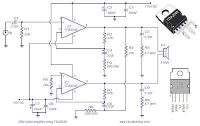
    A 30 watt audio amplifier circuit using TDA2040 is shown here. TDA2040 is a Class AB monolithic integrated audio amplifier available in Pentawatt package. The IC has low harmonic distortion, low cross over distortion and has a built in circuitry for short circuit protection.

    In the circuit two TDA2040 ICs are wired in BTL (Bridge Tied Load) configuration in order to deliver 30W output into an 8 ohm speaker at +/-16V DC supply. Capacitor C1 is the input DC decoupling capacitor. Network comprising of components R2, C4, R3 provides feedback for IC1 while R7, C6, R8 network provides feedback for IC2. Network C5, R5 and C9, R9 provides high frequency stability. Capacitors C2, C3 filters the positive supply rail while capacitors C7, C8 filters the negative supply rail.

    TDA2040 based A 30 watt audio amplifier circuit

    • A well designed and good quality PCB will always improve sound quality.
    • Use +/-16V DC dual supply for powering the amplifier.
    • Heat sinks are necessary for IC1 and IC2.
    • Load can be an 8 ohm speaker.
    • C2, C7 must be rated 25V and other electrolytics can be 10 or 15V.
    S:circuitstoday.com

    TDA2613 using 6 watt audio amplifier circuit(Hi Fi)

    TDA2613 using 6 watt audio amplifier circuit(Hi Fi)

    A 6 watt audio amplifier circuit using TDA2613 is shown here. TDA2613 is an integrated Hi-Fi audio amplifier IC from Philips Semiconductors. The IC is switch ON / switch OFF click proof, short circuit proof, thermally protected and is available in 9 pin single in line plastic package.

    In the given circuit, TDA2613 is wired to operate from a single supply. Capacitor C4 is the input DC decoupler while capacitors C5, C6 are power supply filters. Input audio is fed to the non inverting input through capacitor C4. Inverting input and Vp/2 pins of the IC are tied together and connected to ground through capacitor C3. Capacitor C2 couples the speaker to the ICs output and the network comprising of capacitor C1 and resistor R1 improves the high frequency stability.

    • Assemble the circuit on good quality PCB.
    • Supply voltage (Vs) can be anything between 15 to 24V DC.
    • Heat sink is necessary for TDA2613.
    • Do not give more than 24V to TDA2613.
    S:circuitstoday.com

    How to make a simple Proximity detector or sensor !!!!

    Tags
    How to make a simple Proximity detector or sensor  !!!!

    This is a simple proximity detector using IC CS209. The CS209A is a bipolar monolithic integrated circuit for use in metal detection/proximity sensing applications.The CS209A contains an oscillator set up by an external parallel resonant tank and a feedback resistor connected between pin 2 & 3 .The internal oscillator operates close to the resonant frequency of the tank circuit.As a metal object is brought close to the inductor, the amplitude of the voltage across the tank gradually begins to drop. When the envelope of the oscillation reaches a certain level, the IC causes the outputs to toggle states.potentiometer connected between pin 1 & 8 is adjusted to achieve a certain detection distance range. The larger the resistance the greater the trip-point distance.Detection range can be increased by using a high Q coil.Maximum possible range is 1 inch with a well tuned circuit.Only difficulty in making this circuit is the tuning up the circuit to a particular range.For making it easy place a metal piece at the desired distance from coil (with in 1 inch) and adjust resistance Rf to make one of the outputs ( pin4 or 5) to change state.

    S:circuitstoday.com

    Fire Alarm Circuit (LOW CAST)

    Tags
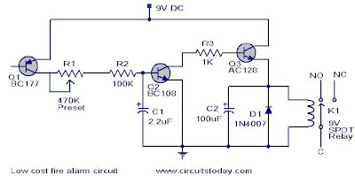
    When there is a fire breakout in the room the temperature increases.This ultra compact and low cost fire alarm senses fire breakout based on this fact.

    Transistor BC177 (Q1) is used as the fire sensor here.When the temperature increases the leakage current of this transistor also increases.The circuit is designed so that when there is an increase in the leakage current of Q1 ,transistor Q2 will get biased.As a result when there is a fire breakout the transistor Q2 will be on.The emitter of Q2 (BC 108)is connected to the base of Q3(AC 128).So when Q2 is ON Q3 will be also ON.The transistor Q3 drives the relay which is used to drive the load ie,light,bell,horn etc as an indication of the fire.The diode D1 is used as a free wheeling diode to protect it from back EMF generated when relay is switched.

    Fire Alarm Circuit (LOW CAST)

    NOTES:

    • The Preset R1 can be used to desired temperature level for setting the alarm ON.
    • This is not a latching alarm,ie;when the temperature in the vicinity of the sensor decreases below the set point the alarm stops.
    • The circuit can be powered using a 9V battery or a 9V battery eliminator.
    • All capacitors are electrolytic and must be rated at least 10V.
    • The load can be connected through the C,NC,NO points of the relay according to your need.
    • The calibration can be done using a soldering iron,and a thermo meter.Switch ON the power supply.Keep the tip of soldering iron near to the Q1.Same time also keep the thermometer close to it.When the temperature reaches your desired value adjust R1 so that relay gets ON.Done!
    • S:circuitstoday.com

    Basic magnetic proximity switch

    Basic magnetic proximity switch

    Here is the circuit diagram of a magnetic proximity switch that finds a lot of applications in many fields.The circuit is based on a magnetic reed switch(S1) as the proximity sensor. A monostable multivibrator based on NE555 (IC1) and a toggle flip flop based on CD4013 (IC2) does the rest of the circuit.

    When a magnet is reached in proximity of S1 it closes to give a negative trigger at pin 2 of IC1.The output of IC1 goes high for a time determines by R2 and C2.This clocks the IC2 wired as a toggle flip flop.The output (pin 1 ) of IC2 goes high and the transistor Q1 is biased to ON.The relay is activated and so do the equipment connected to the relay.The LED D1 glows when IC1 is triggered.

    • Switch S1 can be a general purpose magnetic reed switch.
    • The equipment to control can be connected using NC,NO and C points of the relay according to the application.
    • Use a 12 regulated power supply for powering the circuit.

    The working of a camera (a device that is used to capture and record photos or videos)

    Tags
    The work of a camera – photography is considered to be one of the greatest inventions of mankind. It has not only helped us see the entire world through a click, but has also transformed how people conceive the world. They can also be kept as a remembrance for the rest of our life.

    Camera can be defined as a device that is used to capture and record photos or videos.

    Early use of camera

    Nowadays we see a lot of advanced cameras that are used to capture motion as well as images from a very far distance. During the time of its invention images could be taken only in a room and could not be portable. The instrument should be kept in a dark chamber or box and the room should function as a real-time imaging system. Thus the camera was earlier called “camera-obscura” which meant “dark chamber”. The first of this kind was invented by a scientist called Johannes Kepler. But this apparatus was very huge and could be portable only as a tent. For this instrument to work the light was passed onto it through a convex lens. Thus an image consisting of external objects would be formed which was subjected to the surface of a paper or glass, placed at the focus of the lens. A much compact and portable camera was introduced in 1685 by Johann Zahn.

    After years of work by many prominent people the first colour photo was invented by the famous physicist James Clark Maxwell along with Thomas Sutton. Then came the invention of the video made in cameras during the early 1920s. This technology has eventually grown to such heights that in this 21st century, these ordinary film cameras have been replaced by digital cameras.

    Parts of a camera

    A camera has mainly three parts. They are

    • Mechanical part or the camera body
    • Optical part or the lens section
    • The chemical part or the film

    The way in which these three parts are connected represents the different types of cameras. Thus by combining these three parts and using them under the correct calibration produces a correct picture. They are capable of working in both the visible spectrum as well as in other portions of the electromagnetic spectrum. The basic shape of a camera needs an enclosed hollow chamber with an opening at one end. This opening, also called aperture helps in the entrance of light. This light is the actual image that has to be captured. So a capturing mechanism is set at the other end. All cameras have the lens assembled in the front. This lens helps in capturing the light, which is in turn captured and stored by the recording surface. Most ordinary cameras can take one image at a time. Most video cameras can take a maximum of 24 film frames/sec.

    Mechanism of a camera

    To know the complete mechanism of the camera, it is better to know each and every parameter of the camera.

    1. Focus

    A camera’s focus greatly depends on the clarity of the picture taken. But the focus can be limited only to a certain distance. This range is limited to the range of the lens. This range when adjusted to get a perfect image is called the focus of the camera. For accurate focussing of cameras, the device is comprised of a fixed focus and also consists of a wide-angle lens and a small aperture in front of the camera. The range of focus will be clearly indicated in the camera with symbols like two people standing upright, mountains and so on. For a simple camera, a reasonable focus of about 3 meters to infinity is available. The focus available on each camera is different. Single-lens reflex (SLR) cameras have a focus that can be changed according to our like. This is done by providing a objective lens and a moving mirror so as to projecting the image to a ground glass or plastic micro-prism screen. Similarly each camera has different settings which will be explained briefly later.

    • The focus of a camera depends on two main features. They are
    • The structure and position of the lens.
    • The angle in which the light beams enter into the lens.

    Consider a pencil kept at a short distance from the lens. When the distance is altered, that is kept near and then farther away from the lens, the angle of entry of the light changes accordingly. This light is hit on the film surface kept inside the camera. The angle becomes sharper when the image is close to the lens and will become narrower when the image is kept far away. Thus when the lens is focused farther and then nearer from the pencil, the image is actually moving closer or farther away from the film surface. The correct image will be obtained when the focus is adjusted in such a way that you can line up the focused real image of an object so it falls directly on the film surface.

    The working of a camera (a device that is used to capture and record photos or videos)

    2. Camera Lens

    The quality of the photograph taken largely depends on the type of lens used. The precision of a lens depends on a factor called “bending angle”. This in turn, depends on the structure of the lens. If the lens has a flat shape, the bending angle is less. Thus the light beams will converge a little distance farther away from the lens. Thus the image is also formed farther away. Thus when the distance increases, the size of the image also increases, though the size of the film is constant. If the lens has a round shape, the bending angle will be high. Thus the image will be formed a lot more nearer to the lens.

    Costly cameras have a lot of lenses, which are replaced or combined according to the magnification required. This magnification power of a lens is called the focal length. Greater the focal length, greater the magnification.

    3. Camera Film

    For an image to be recorded and viewed it must be stored in a film. When an image is captured, it is actually being “chemically” recorded onto a film. The film mainly consists of millions of light-sensitive grains, which are suspended on a plastic strip. These grains chemically react, when exposed to light. This reaction causes the image to be recorded on the film. This film is then developed by reacting it with other chemicals. For black and white films, the chemicals cause the grains to appear darker when exposed to light. Thus, the darker areas appear lighter and the lighter areas appear darker. This is reversed while printing out the photos.

    For producing colour films, the film consists of light sensitive materials that respond to colours red, green and blue. When they are washed and chemically reacted, you get a negative of a colour photo.

    Different camera designs

    There are a lot of types of cameras like Plate camera, large format camera, medium format camera, folding camera, rangefinder camera and so on. Out of these the most used ones are the single-lens reflex camera (SLR) and the point and shoot camera. The difference comes in the manner in which the photographer visualizes the scene. In a point and shoot camera, you do not see the real image through the camera lens. Instead, you get to see only a blurred vision of the image.

    In an SLR camera, you can see the real image of the scee you are about to capture. It has the same configuration as that of a periscope. When the image is seen from the lens, it hits the lower mirror and bounces from there. It then hits the prism. This prism flips the image to form the original image. The mirror and translucent screen help in providing the exact image to the photographer. Thus, you can focus and compose the image so as to get the exact picture you have in mind.

    The working of a camera (a device that is used to capture and record photos or videos)

    With upcoming technology, the point and shoot cameras are nowadays fully automatic. SLR is built with both manual and automatic controls. The only difference between the manual and automatic cameras is that the former will be controlled by a central processor, instead of the photographer.

    The focus system and the light meter transmit the signals to the microprocessor and thus activate all the motors accordingly. These motors control the adjusting lens and also open and close the aperture.

    S:circuitstoday.com

    Advertisement