Showing posts with label Tutorial. Show all posts

Comprehensive diode clamping circuits

In this article, the working of a clamping circuit is explained. The working of different clamping circuits like positive and negative clamper, with circuit diagrams and waveforms are given below.

A clamping circuit is used to place either the positive or negative peak of a signal at a desired level. The dc component is simply added or subtracted to/from the input signal. The clamper is also referred to as an IC restorer and ac signal level shifter.

In some cases, like a TV receiver, when the signal passes through the capacitive coupling network, it loses its dc component. This is when the clamper circuit is used so as to re-establish the the dc component into the signal input. Though the dc component that is lost in transmission is not the same as that introduced through a clamping circuit, the necessity to establish the extremity of the positive or negative signal excursion at some reference level is important.

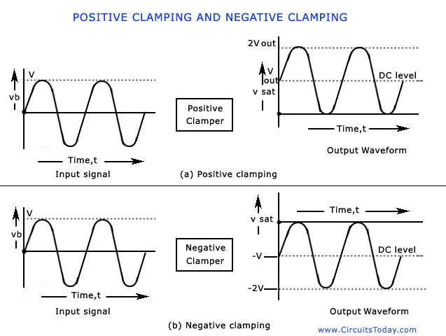
A clamp circuit adds the positive or negative dc component to the input signal so as to push it either on the positive side, as illustrated in figure (a) or on the negative side, as illustrated in figure (b).

The circuit will be called a positive clamper , when the signal is pushed upward by the circuit. When the signal moves upward, as shown in figure (a), the negative peak of the signal coincides with the zero level.

The circuit will be called a negative clamper, when the signal is pushed downward by the circuit. When the signal is pushed on the negative side, as shown in figure (b), the positive peak of the input signal coincides with the zero level.

Comprehensive diode clamping circuits

Comprehensive diode clamping circuits

For a clamping circuit at least three components — a diode, a capacitor and a resistor are required. Sometimes an independent dc supply is also required to cause an additional shift. The important points regarding clamping circuits are:

(i) The shape of the waveform will be the same, but its level is shifted either upward or downward,

(ii) There will be no change in the peak-to-peak or rms value of the wave­form due to the clamping circuit. Thus, the input waveform and output waveform will have the same peak-to-peak value that is, 2Vmax. This is shown in the figure above. It must also be noted that same readings will be obtained in the ac voltmeter for the input voltage and the clamped output voltage.

(iii) There will be a change in the peak and average values of the waveform. In the figure shown above, the input waveform has a peak value of Vmax and average value over a complete cycle is zero. The clamped output varies from 2 Vmax and 0 (or 0 and -2Vmax). Thus ths peak value of the clamped output is 2Vmax and average value is Vmax.

(iv) The values of the resistor R and capacitor C affect the waveform.

(v) The values for the resistor R and capacitor C should be determined from the time constant equation of the circuit, t = RC. The values must be large enough to make sure that the voltage across the capacitor C does not change significantly during the time interval the diode is non-conducting. In a good clamper circuit, the circuit time constant t = RC should be at least ten times the time period of the input signal voltage.

It is advantageous to first consider the condition under which the diode becomes forward biased.

Clamping circuits are often used in television receivers as dc restorers. The signal that is sent to the TV receiver may lose the dc components after being passed through capacitively coupled amplifiers. Thus the signal loses its black and white reference levels and the blanking level. Before passing these signals to the picture tube, these reference levels have to be restored. This is done by using clamper circuits. They also find applications in storage counters, analog frequency meter, capacitance meter, divider and stair-case waveform generator.

Consider a negative clamping circuit, a circuit that shifts the original signal in a vertical downward direction, as shown in the figure below. The diode D will be forward biased and the capacitor C is charged with the polarity shown, when an input signal is applied. During the positive half cycle of input, the output voltage will be equal to the barrier potential of the diode, V0 and the capacitor is charged to (V – VQ). During the negative half cycle, the diode becomes reverse-biased and acts as an open-circuit. Thus, there will be no effect on the capacitor voltage. The resistance R, being of very high value, cannot discharge C a lot during the negative portion of the input wave­form. Thus during negative input, the output voltage will be the sum of the input voltage and the capacitor voltage and is equal to – V – (V — V0) or – (2 V – V0). The value of the peak-to-peak output will be the difference of the negative and positive peak voltage levels is equal to V0-[-(2V-V0)] or 2 V.

The figure shown below can me modified into a positive clamping circuit by reconnecting the diode with reversed polarity. The positive clamping circuit moves the original signal in a vertical upward direction. A positive clamping circuit is shown in the figure below. It contains a diode D and a capacitor C as are contained in a negative clamper. The only difference in the circuit is that the polarity of the diode is reversed. The remaining explanation regarding the working of the circuit is the same as it is explained for the negative clamper.

To remember which way the dc level of a signal moves, look at figure shown below. Notice that the diode arrows point downward, the same direction as the dc shift.

Comprehensive diode clamping circuits

Similarly in the figure shown below, the diode arrow points upward, again the same direction as the dc shifts. It means that, when the diode points upward. We have a positive dc clamper and when the diode points downward, the circuit is a negative dc clamper.


Comprehensive diode clamping circuits

A number of clamping circuits with their effect on the input signal are shown in the figure given below. All the figures shown below have the input and output signals in square waves, the same procedure can be used for sinusoidal inputs. In fact, one approach to the analysis of clamping networks with sinusoidal inputs is to replace the sinusoidal wave signal by a square wave of the same peak values. The resulting output will then form an envelope for the sinusoidal response, as illustrated in figure (g) for a network appearing in figure (f). The diodes have been assumed to be ideal and 5 RC » T/2 in drawing the output wave­forms


Comprehensive diode clamping circuitsComprehensive diode clamping circuits
Comprehensive diode clamping circuitsS:circuitstoday.com

A complete basic tutorial for 555 timer IC

This article covers every basic aspect of 555 Timer IC. You may already know that SE/NE 555 is a Timer IC introduced by Signetics corporation in 1970′s. In this article we cover the following information about 555 Timer IC.

1. Introduction to 555 Timer IC

2. 555 Timer IC Pin Configuration

3. Basics of 555 Timer

4. Block Diagram

5. Working Principle

6. Download Data Sheet

1. Introduction

A complete basic tutorial for 555 timer IC

One of the most versatile linear ICs is the 555 timer which was first introduced in early 1970 by Signetic Corporation giving the name as SE/NE 555 timer. This IC is a monolithic timing circuit that can produce accurate and highly stable time delays or oscillation. Like other commonly used op-amps, this IC is also very much reliable, easy to use and cheaper in cost. It has a variety of applications including monostable and astable multivibrators, dc-dc converters, digital logic probes, waveform generators, analog frequency meters and tachometers, temperature measurement and control devices, voltage regulators etc. The timer basically operates in one of the two modes either as a monostable (one-shot) multivibrator or as an astable (free-running) multivibrator.The SE 555 is designed for the operating temperature range from – 55°C to 125° while the NE 555 operates over a temperature range of 0° to 70°C.

The important features of the 555 timer are :

  • It operates from a wide range of power supplies ranging from + 5 Volts to + 18 Volts supply voltage.
  • Sinking or sourcing 200 mA of load current.
  • The external components should be selected properly so that the timing intervals can be made into several minutes Proper selection of only a few external components allows timing intervals of several minutes along with the frequencies exceeding several hundred kilo hertz.
  • It has a high current output; the output can drive TTL.
  • It has a temperature stability of 50 parts per million (ppm) per degree Celsius change in temperature, or equivalently 0.005 %/ °C.
  • The duty cycle of the timer is adjustable with the maximum power dissipation per package is 600 mW and its trigger and reset inputs are logic compatible.

2. IC Pin Configuration

A complete basic tutorial for 555 timer IC

The 555 Timer IC is available as an 8-pin metal can, an 8-pin mini DIP (dual-in-package) or a 14-pin DIP.

This IC consists of 23 transistors, 2 diodes and 16 resistors. The explanation of terminals coming out of the 555 timer IC is as follows. The pin number used in the following discussion refers to the 8-pin DIP and 8-pin metal can packages.

A complete basic tutorial for 555 timer IC

Pin 1: Grounded Terminal: All the voltages are meas­ured with respect to this terminal.

Pin 2: Trigger Terminal: This pin is an inverting input to a comparator that is responsible for transition of flip-flop from set to reset. The output of the timer depends on the amplitude of the external trigger pulse applied to this pin.

Pin 3: Output Terminal: Output of the timer is avail­able at this pin. There are two ways in which a load can be connected to the output terminal either between pin 3 and ground pin (pin 1) or between pin 3 and supply pin (pin 8). The load connected between pin 3 and ground supply pin is called the normally on load and that connected between pin 3 and ground pin is called the normally off load.

Pin 4: Reset Terminal: To disable or reset the timer a negative pulse is applied to this pin due to which it is referred to as reset terminal. When this pin is not to be used for reset purpose, it should be connected to + VCC to avoid any possibility of false triggering.

Pin 5: Control Voltage Terminal: The function of this terminal is to control the threshold and trigger levels. Thus either the external voltage or a pot connected to this pin determines the pulse width of the output waveform. The external voltage applied to this pin can also be used to modulate the output waveform. When this pin is not used, it should be connected to ground through a 0.01 micro Farad to avoid any noise problem.

Pin 6: Threshold Terminal: This is the non-inverting input terminal of comparator 1, which compares the voltage applied to the terminal with a reference voltage of 2/3 VCC. The amplitude of voltage applied to this terminal is responsible for the set state of flip-flop.

Pin 7 : Discharge Terminal: This pin is connected internally to the collector of transistor and mostly a capacitor is connected between this terminal and ground. It is called discharge terminal because when transistor saturates, capacitor discharges through the transistor. When the transistor is cut-off, the capacitor charges at a rate determined by the external resistor and capacitor.

Pin 8: Supply Terminal: A supply voltage of + 5 V to + 18 V is applied to this terminal with respect to ground (pin 1).

3. 555 Timer Basics

The 555 timer combines a relaxation oscillator, two comparators, an R-S flip-flop, and a discharge capacitor.

R-S Flip-Flop: – A pair of cross-coupled transistors is shown in figure. Each collector drives the opposite base through resistance RB. In such circuit one transistor is saturated while the other is cut-off. For instance, if transistor Q1 is saturated, its collector voltage is almost zero. So there is no base drive for transistor Q2 and it goes into cut-off and its collector voltage approaches + VCC. This high voltage produces enough base current to keep transistor Q1 in saturation.

On the other hand if transistor Q1 is cut-off, its collector voltage, which is approximately equal to + VCC, drives the transistor Q2 into saturation. The low collector voltage (which is approximately to zero) of this transistor then keeps the transistor Q2 in cut-off.Depending on which transistor is saturated, the Q output is either low or high. By adding more components to the circuit, an R-S flip-flop is obtained. R-S flip-flop is a circuit that can set the Q output to high or reset it low. Incidentally, a complementary (opposite) output Q is available from the collector of the other transistor.

Figure shows the schematic symbol for an R-S flip-flop of any design. The circuit latches in either two states. A high S input sets Q to high; a high R input resets Q to low. Output Q remains in a given state until it is triggered into the opposite state.

A complete basic tutorial for 555 timer IC

Basic Timing Concept

Figure illustrates some basic ideas that will prove useful in coming blog posts of the 555 timer. Assuming output Q high, the transistor is saturated and the capacitor voltage is clamped at ground i.e. the capacitor C is shorted and cannot charge.

The non-inverting input voltage of the comparator is referred to as the threshold voltage while the inverting input voltage is referred to as the control voltage. With R-S flip flop set, the saturated transistor holds the threshold voltage at zero. The control voltage, however, is fixed at 2/3 VCC (i.e. at 10 V) because of the voltage divider.

Suppose that a high voltage is applied to the R input. This resets the flip-flop R-Output Q goes low and the transistor is cut-off. Capacitor C is now free to charge. As this capacitor C charges, the threshold voltage rises. Eventually, the threshold voltage becomes slightly greater than (+ 10 V). The output of the comparator then goes high, forcing the R S flip-flop to set. The high Q output saturates the transistor, and this quickly discharges the capacitor. The two waveforms are depicted in figure. An exponential rise is across the capacitor C, and a positive going pulse appears at the output Q. Thus capacitor voltage VC is exponential while the output is rectangular, as illustrated in figure.

4. Block Diagram

A complete basic tutorial for 555 timer IC

The block diagram of a 555 timer is shown in the above figure. A 555 timer has two comparators, which are basically 2 op-amps), an R-S flip-flop, two transistors and a resistive network.

  • Resistive network consists of three equal resistors and acts as a voltage divider.
  • Comparator 1 compares threshold voltage with a reference voltage + 2/3 VCC volts.
  • Comparator 2 compares the trigger voltage with a reference voltage + 1/3 VCC volts.

Output of both the comparators is supplied to the flip-flop. Flip-flop assumes its state according to the output of the two compa­rators. One of the two transistors is a discharge transis­tor of which collector is connected to pin 7. This tran­sistor saturates or cuts-off according to the output state of the flip-flop. The saturated transis­tor provides a discharge path to a capacitor con­nected externally. Base of another transistor is connected to a reset terminal. A pulse applied to this terminal resets the whole timer irrespective of any input.

5. Working Principle

Refer Block Diagram of 555 timer IC given above:

Comparator 1 has a threshold input (pin 6) and a control input (pin 5). In most applications, the control input is not used, so that the control voltage equals +2/3 VCC. Output of this comparator is applied to set (S) input of the flip-flop. Whenever the threshold voltage exceeds the control voltage, comparator 1 will set the flip-flop and its output is high. A high output from the flip-flop saturates the discharge transistor and discharge the capacitor connected externally to pin 7. The complementary signal out of the flip-flop goes to pin 3, the output. The output available at pin 3 is low. These conditions will prevail until comparator 2 triggers the flip-flop. Even if the voltage at the threshold input falls below 2/3 VCC, that is comparator 1 cannot cause the flip-flop to change again. It means that the comparator 1 can only force the flip-flop’s output high.

To change the output of flip-flop to low, the voltage at the trigger input must fall below + 1/3 Vcc. When this occurs, comparator 2 triggers the flip-flop, forcing its output low. The low output from the flip-flop turns the discharge transistor off and forces the power amplifier to output a high. These conditions will continue independent of the voltage on the trigger input. Comparator 2 can only cause the flip-flop to output low.

From the above discussion it is concluded that for the having low output from the timer 555, the voltage on the threshold input must exceed the control voltage or + 2/3 VCC. They also turn the discharge transistor on. To force the output from the timer high, the voltage on the trigger input must drop below +1/3 VCC. This also turns the discharge transistor off.

A voltage may be applied to the control input to change the levels at which the switching occurs. When not in use, a 0.01 nano Farad capacitor should be connected between pin 5 and ground to prevent noise coupled onto this pin from causing false triggering.

Connecting the reset (pin 4) to a logic low will place a high on the output of flip-flop. The discharge transistor will go on and the power amplifier will output a low. This condition will continue until reset is taken high. This allows synchronization or resetting of the circuit’s operation. When not in use, reset should be tied to +VCC.

S:circuitstoday.com

Advertisement