Taken alone, amplifier characteristics of the voice of the PA300, which is not revolutionary. A powerful 300-watt Hi-Fi amplifier, which is not difficult to make, but in combination, showing something special.
There are some guidelines for the design of power amplifier: Pure-Fi hello without compromise. Simplicity and reliability. High power. The current design of the sound reproduction a mixture thereof. The result is a unit which does not esoteric components do not use too complicated, easily gives somewhat. In fact, it would be called good "Hi-fi amplifier sound system."
There will be a few eyebrows at a power of 300 watts (4 ohm), where, of course, that in the living average 30-40 watts per channel is more than enough. However, the peaks are reproduced in the power of music 10-20 times the normal level. This means that some of the required power reserve. There are also speakers with such low efficiency to the need for much more than 30-40W. And last but not least, there are a lot of people who want the amplifier is much greater than the average living room to the room, such as amateur music hall.
 Fig. 1. With the exception of an IC at the input, the circuit of the PA300 amplifier is conventional.
Straightforward designSince every amplifier contains a certain number of standard components, the circuit of Fig.1 will look pretty familiar to most audio enthusiasts. Two aspects may hit the eye: the higher than usual supply voltage and the presence of a couple of ics. The first is to be expected in view of the power output. One of the ics is not in the signal path and this immediately points to it being part of a protection circuit. What is unconventional is an IC in the input stage. Normally, this stage consists of a differential amplifier followed by a voltage amplifier of sorts, often also a differential amplifier, to drive the predriver stages. In the PA300, the entire input stage is contained in one ic, a Type NE5534 (IC1).
The internal circuit of IC1 is shown in the box on further on in this article. It may also be of interest to note that the NE5534 is found in nine out of every ten cd players(as amplifier in the analogue section). This is reflected in its price which is low. Its only drawback is that its supply voltage is far below that of the remainder of the amplifier.
This means an additional symmetrical supply of ±15 V. Moreover, it restricts the drive capability of the input stage. The supply requirement is easily met with the aid of a couple of zener diodes and resistors. The drive restriction means that the amplifier must provide a measure of voltage amplification after the input stage.
Circuit description
The input contains a high-pass filter, C5-R3 and a low-pass filter, R2-C6. The combination of these filters limits the bandwidth of the input stage to a realistic value: it is not necessary for signals well outside the audio range to be amplified – in fact, this may well give rise to difficulties.
Opamp IC1 is arranged as a differential amplifier; its non-inverting (+) input functions as the meeting point for the overall feedback. The feedback voltage, taken from junction D7-D8, is applied to junction R4-R5 via R9. Any necessary compensation is provided by C9, C12 and C14. The voltage amplification is determined by the ratio R9:R5, which in the present circuit is x40.
The output of IC1 is applied to drive stages T1 and T3 via R6. These transistors operate in Class A: the current drawn by them is set to 10 mA by voltage divider R10- R13 and their respective emitter resistors. Their voltage and current amplification is appreciable, which is as required for the link between the input and output stages. The output amplifier proper consists of drive stages T6 and T7 and power transistors T8, T9, T14, T15. which have been arranged as symmetrical power darlingtons. Because of the high power, the output transistors are connected in parallel. The types used can handle a collector current of 20 A and have a maximum dissipation of 250 W.
The output stages operate in Class AB to ensure a smooth transition between the n-p-n and p-n-p transistors, which prevents cross-over distortion. This requires a small current through the power transistors, even in the absence of an input signal. This current is provided by 'zener' transistor T2, which puts a small voltage on the bases of T6 and T7 so that these transistors just conduct in quiescent operation. The level of the quiescent current is set accurately with P1.
To ensure maximum thermal stability, transistors T1–T3 and T6–T7 are mounted on and the same heat sink. This keeps the quiescent current within certain limits. With high drive signals, this current can reach a high level, but when the input signal level drops, the current will diminish only slowly until it has reached its nominal value.
Diodes D7, D8 protect the output stages against possible counter voltages generated by the complex load. Resistor R30 and capacitor C17 form a Boucherot network to enhance the stability at high frequencies. Inductor L1 prevents any problems with capacitive loads (electrostatic loudspeakers). Resistor R29 ensures that the transfer of rectangular signals are not adversely affected by the inductor.
Protection circuitsAs any reliable amplifier, the PA300 is provided with adequate protection measures.
These start with fuses F1 and F2, which guard against high currents in case of overload or short-circuits. Since even fast fuses are often not fast enough to prevent the power transistors giving up the ghost in such circumstances, an electronic short-circuit protection circuit, based on T4 and T5, has been provided. When, owing to an overload or short-circuit, very high currents begin to flow through resistors R25 and R27, the potential drop across these resistors will exceed the base-emitter threshold voltage of T4 and T5. These transistors then conduct and short-circuit or reduce drive signal at their bases. The output current then drops to zero. If a direct voltage appears at the output terminals, or the temperature of the heat sink rises unduly, relay Re1 removes the load from the output. The loudspeakers are also disconnected by the relay when the mains is switched on (power-on delay) to prevent annoying clicks and plops.
The circuits that make all this possible consist of dual comparator IC2, transistors T10–T13, and indicator diodes D13 and D14. They are powered by the 15 V line provided by zener diode D10 and resistor R42.
The 'ac' terminal on the PCB is linked to one of the secondary outputs on the mains transformer. As soon as the mains is switched on, an alternating voltage appears at that terminal, which is rectified by D12 and applied as a negative potential to T12 via R50. The transistor will then be cut off, so that C20 is charged via R36 and R44. As long as charging takes place, the inverting (+) input of comparator IC2b is low w.r.t. the non-inverting (–) input. The output of IC2b is also low, so that T13 is cut off and the relay is not energized. This state is indicated by the lighting of D13. When C20 has been charged fully, the comparator changes state, the relay is energized (whereupon D13 goes out) and the loudspeakers are connected to the output. When the mains is switched off, the relay is deenergized instantly, whereupon the loudspeakers are disconnected so that any switch-off noise is not audible.
The direct-voltage protection operates as follows. The output voltage is applied to T10 and T11 via potential divider R32-R34. Alternating voltages are short-circuited to ground by C18. However, direct voltages greater than +1.7 V or more negative than –4.8V switch on T10 or T11 immediately. This causes the +ve input of IC2a to be pulled down, whereupon this comparator changes state, T13 is cut off, and the relay is deenergized. This state is again indicated by the lighting of D13.
Strictly speaking, temperature protection is not necessary, but it offers that little bit extra security. The temperature sensor is R39, a ptc (positive temperature coefficient) type, which is located on the board in a position where it rests against the rectangular bracket. Owing to a rising temperature, the value of R39 increases until the potential at the –ve input of IC2a rises above the level at the +ve input set by divider R45-R46, whereupon the output of IC2a goes low. This causes IC2b to change state, whereupon T13 is cut off and the relay is deenergized. This time, the situation is indicated by the lighting of D14. The circuit has been designed to operate when the temperature of the heat sink rises above 70 °C. Any relay clatter may be obviated by reducing the value of R48.
The terminal marked 'CLIP' on the PCB is connected to the output of IC1 via R31. It serves to obtain an external overdrive indication, which may be a simple combination of a comparator and LED. Normally, this terminal is left open.
Power supply
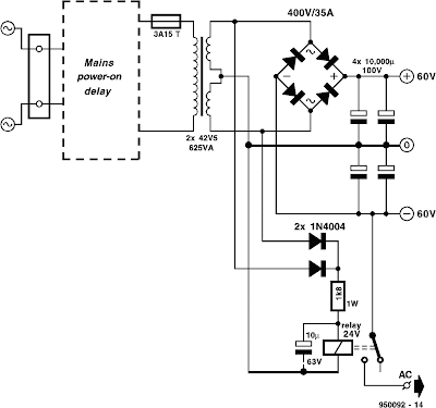
As with most power amplifiers, the ±60 V power supply need not be regulated. Owing to the relatively high power output, the supply needs a fairly large mains transformer and corresponding smoothing capacitors—see Fig. 2. Note that the supply shown is for a mono amplifier; a stereo outfit needs two supplies.

Fig. 2. The power supply is straightforward, but can handle a large current. Voltage 'ac'serves as drive for the power-on delay circuit.
The transformer is a 625 VA type, and the smoothing capacitors are 10 000 µF, 100 V electrolytic types. The bridge rectifier needs to be mounted on a suitable heat sink or be mounted directly on the bottom cover of the metal enclosure.. The transformer needs two secondary windings, providing 42.5 V each. The prototype used a toroidal transformer with 2x40 V secondaries. The secondary winding of this type of transformer is easily extended: in the prototype 4 turns were added and this gave secondaries of 2x42.5 V.
The box 'Mains power-on delay' provides a gradual build-up of the mains voltage, which in a high-power amplifier is highly advisable. A suitable design was published in 305 Circuits (page 115).
The relay and associated drive circuit is intended to be connected to terminal 'ac' on the board, where it serves to power the power-on circuit. If a slight degradation of the amplifier performance is acceptable, this relay and circuit may be omitted and the PCB terminal connected directly to one of the transformer secondaries.
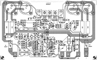
Fig. 3. Component layout of the printed-circuit board for the 300 W power amplifier.
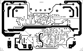
Fig. 4. Track layout of the printed-circuit board for the 300 W power amplifier.
ConstructionBuilding the amplifier is surprisingly simple. The printed-circuit board in Fig. 4 is well laid out and provides ample room. Populating the board is as usual best started with the passive components, then the electrolytic capacitors, fuses and relay. There are no 'difficult' parts.
Circuits IC1 and IC2 are best mounted in appropriate sockets. Diodes D13 and D14 will, of course, have to be fitted on the front panel of the enclosure and are connected to the board by lengths of flexible circuit wire. Inductor L1 is a DIY component; i consists of 15 turns of 1 mm. dia. enamelled copper wire around R29 (not too tight!). Since most of the transistors are to be mounted on and the same heat sink, they are all located at one side of the board. However, they should first be fitted on a rectangular bracket, which is secured to the heat sink and the board—see Fig. 3. Note that the heat sink shown in this photograph proved too small when 4 Ohm loudspeakers were used. With 8 Ohm speakers, it was just about all right, but with full drive over sustained periods, the temperature protection circuits were actuated. If such situations are likely to be encountered, forced cooling must be used. As already stated, temperature sensor R39 should rest (with its flat surface) against the rectangular bracket. On the board, terminals 'A' and 'B' terminals to the left of R39 must be connected to 'A' and 'B' above IC2 with a twisted pair of lengths of insulated circuit wire as shown in Fig. 3. The points where to connect the loudspeaker leads and power lines are clearly marked on the board. Use the special flat AMP connectors for this purpose: these have large-surface contacts that can handle large currents. The loudspeaker cable should have a cross-sectional area of not less than 2.5 mm2.
FinallyHow the amplifier and power supply are assembled is largely a question of individual taste and requirement. The two may be combined into a mono amplifier, or two each may be built into a stereo amplifier unit. Our preference is for mono amplifiers, since these run the least risk of earth loops and the difficulties associated with those. It is advisable to make the '0' of the supply the centre of the earth connections of the electrolytic capacitors and the centre tap of the transformer.
The single earthing point on the supply and the board must be connected to the enclosure earth by a short, heavy-duty cable. This means that the input socket must be an insulated type. This socket must be linked to the input on the board via screened cable.
To test the amplifier, turn P1 fully anticlockwise and switch on the mains. After the output relay has been energized, set the quiescent current. This is done by connecting a multimeter (direct mV range) across one of resistors R25–R28 and adjusting P1 until the meter reads 27 mV (which corresponds to a current of 100 mA through each of the four power transistors). Leave the amplifier on for an hour or so and then check the voltage again: adjust P1 as required.


