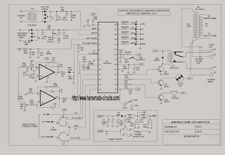
The proposed sinewave inverter UPS circuit is built using PIC16F72 microcontroller, some passive electronic components and associated power devices.
Main Features:
The main technical features of the discussed PIC16F72 sinewave inverter may be evaluated from the following data:
Power output (625/800va) fully customization and can be upgraded to other desired levels.
Battery 12V/200AH
Inverter Output Volt : 230v (+2%)
Inverter Output Frequency : 50Hz
Inverter Output Waveform : PWM Modulated Sinewave
Harmonic Distortion : less than 3%
Crest Factor : less than 4:1
Inverter efficiency : 90% For 24v System, around 85% with 12v System
Audible Noise : less 60db At 1-meter
Inverter Protection Features
Low-battery Shut-down
Overload Shut-down
Output Short Circuit Shut-down
Low-battery Detection and Shutdown Feature
Beep Start initiated at 10.5v (beep At Every 3-sec)
Inverter Shut-down at around 10v (5 pulses of beep in every 2-sec)
Over Load : Beep Initiated at 120% Load (beep at the rate of 2-sec)
Inverter Shut-down at 130% Overload (5 pulses of beep in every 2-sec)
LED Indicators are provided for the following:
Inverter On
Low-battery - Flashing in Low battery mode with Alarm
Solid ON During Cut-OFF
Over Load - Flashing at Overload cut-off with Alarm
Solid ON During Cut-OFF
Charging mode - Flashing at Charging mode
Solid ON During Absorption
Mains Indication - LED On
Circuit Specifications
8-bit Microcontroller Based Control Circuit
H-bridge Inverter Topology
Mosfet Switching Fault Detection
Charging Algorithm : Mosfet PWM based switch mode Charger Controller 5-amp/15-amp
2-step Charging Step-1: Boost Mode (led Flash)
Step-2: Absorption Mode (led On)
DC Fan initialization for Internal Cooling During Charging/inv Operation
circuit diagram
The following explanation provides the details of the various circuit stages involved in the design:
In Inverter Mode
As soon as mains fails, the battery logic is detected at pin#22 of the IC which instantly prompts the controller section to switch the system in the inverter/battery mode.
In this mode the controller begins generating the required PWMs via its pin#13 (ccp out), however the PWM generation rate is implemented only after the controller confirms the logic level at pin#16 (INV/UPS switch).
If a high logic is detected at this pin (INV mode) the controller initiates a fully modulated duty cycle which is around 70%, and in case of a low logic at the indicated pinout of the IC, then the controller may be prompted to generate burst of PWMs ranging from 1% to 70% at a rate of 250mS period, which is termed as soft delay output while in the UPS mode.
The controller simultaneously with the PWMs also generates a "channel select" logic through pin#13 of the PIC which is further applied to pin#8 of the IC CD4081.
Throughout initial time period of the pulse (i.e 10ms) the pin12 of the PWM controller is rendered high such that the PWM can be obtained from pin10 of CD4081 exclusively and after 10mS, pin14 of controller is logic high and the PWM is accessible from pin11 of CD4081, as a result using this method a pair of anti-phased PWM becomes accessible to switch on the MOSFETs.
Aside from that a high logic (5V) becomes accessible from pin11 of the PWM controller, this pin turns high each time inverter is ON and ends up being low whenever inverter is OFF. This high logic is applied to pin10 of each the MOSFET drivers U1 and U2, (HI pin) to activate the high side MOSFETs of the two the mosfet banks.
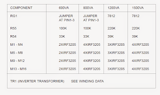
For upgrading the proposed Sinewave UPS using PIC16F72, the following data may be used and implemented appropriately.
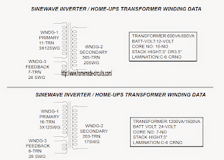
The following data supplies the full transformer winding details:


