example of a relaxation oscillator(The op-amp triangular-wave generator)
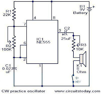
(practice Ham Radio) CW practice oscillator
A circuit diagram that can be used for the generation of CW Morse code is shown here.This circuit can be very useful those who would like practice Ham Radio.The circuit is nothing but an astable multivibrator based on NE 555.The frequency of oscillations of the circuit depends on the components R1,R2 & C1.The circuit can be powered from a 9V PP3 battery.
Notes:
- The POT R2 can be used for frequency adjustments.
- POT R3 can be used for volume adjustments.
- The switch S1 can be a Morse code key.
S:circuitstoday.com
Very Low Power 32kHz Oscillator
Circuit diagram:
The base of T1 is biased at 1.25 V using R5/R4 and the reference in IC1. T1 may be any small-signal transistor with a decent beta of 100 or so at 5 µA (defined here by R3, fixing the collector voltage at about 1 V below Vcc). The amplifier’s nominal gain is approximately 2 V/V. The quartz crystal combined with load capacitors C1 and C3 forms a feedback path around T1, whose 180 degrees of phase shift causes the oscillation. The bias voltage of 1.25 V for the comparator inside the MAX931 is defined by the reference via R2. The comparator’s input swing is thus accurately centred around the reference voltage.
Operating at 3 V and 32 kHz, IC1 draws just 7 µA. The comparator output can source and sink 40 mA and 5 mA respectively, which is ample for most low-power loads. However, the moderate rise/fall times of 500 ns and 100 ns respectively can cause standard, high-speed CMOS logic to draw higher than usual switching currents. The optional 74HC14 Schmitt trigger shown at the circuit output can handle the comparator’s rise/fall times with only a small penalty in supply current.
Author: D. Prabakaran - Copyright: 2004 Elekto
Transistor Schmitt Trigger Oscillator
The Schmitt Trigger oscillator below employs 3 transistors, 6 resistors and a capacitor to generate a square waveform. Pulse waveforms can be generated with an additional diode and resistor (R6). Q1 and Q2 are connected with a common emitter resistor (R1) so that the conduction of one transistor causes the other to turn off. Q3 is controlled by Q2 and provides the squarewave output from the collector.

In operation, the timing capacitor charges and discharges through the feedback resistor (Rf) toward the output voltage. When the capacitor voltage rises above the base voltage at Q2, Q1 begins to conduct, causing Q2 and Q3 to turn off, and the output voltage to fall to 0. This in turn produces a lower voltage at the base of Q2 and causes the capacitor to begin discharging toward 0. When the capacitor voltages falls below the base voltage at Q2, Q1 will turn off causing Q2 and Q3 to turn on and the output to rise to near the supply voltage and the capacitor to begin charging and repeating the cycle. The switching levels are established by R2,R4 and R5. When the output is high, the voltage at the base of Q2 is determined by R4 in parallel with R5 and the combination in series with R2. When the output is low, the base voltage is set by R4 in parallel with R2 and the combination in series with R5. This assumes R3 is a small value compared to R2. The switching levels will be about 1/3 and 2/3 of thesupply voltage if the three resistors are equal (R2,R4,R5).
There are many different combinations of resistor values that can be used. R3 should low enough to pull the output signal down as far as needed when the circuit is connected to a load. So if the load draws 1mA and the low voltage needed is 0.5 volts, R3 would be 0.5/.001 = 500 ohms (510 standard). When the output is high, Q3 will supply current to the load and also current through R3. If 10 mA is needed for the load and the supply voltage is 12, the transistor current will be 24 mA for R3 plus 10 mA to the load = 34 mA total. Assuming a minimum transistor gain of 20, the collector current for Q2 and base current for Q3 will be 34/20 = 1.7 mA. If the switching levels are 1/3 and 2/3 of the supply (12 volts) then the high level emitter voltage for Q1 and Q2 will be about 7 volts, so the emitter resistor (R1) will be 7/0.0017 = 3.9K standard. A lower value (1 or 2K) would also work and provide a little more base drive to Q3 than needed. The remaining resistors R2, R4, R5 can be about 10 times the value of R1, or something around 39K.
The combination of the capacitor and the feedback resistor (Rf) determines the frequency. If the switching levels are 1/3 and 2/3 of the supply, the half cycle time interval will be about 0.693*Rf*C which is similar to the 555 timer formula. The unit I assembled uses a 56K and 0.1 uF cap for a positive time interval of about 3.5 mS. An additional 22K resistor and diode were used in parallel with the 56K to reduce the negative time interval to about 1 mS.
In the diagram, T1 represents the time at which the capacitor voltage has fallen to the lower trigger potential (4 volts at the base of Q2) and caused Q1 to switch off and Q2 and Q3 to switch on. T2 represents the next event when the capacitor voltage has risen to 8 volts causing Q2 an Q3 to turn off and Q1 to conduct. T3 represents the same condition as T1 where the cycle begins to repeat. Now, if you look close on a scope, you will notice the duty cycle is not exactly 50% This is due to the small base current of Q1 which is supplied by the capacitor. As the capacitor charges, the E/B of Q1 is reverse biased and the base does not draw any current from the capacitor so the charge time is slightly longer than the discharge. This problem can be compensated for with an additional diode and resistor as shown (R6) with the diode turned around the other way.
Source
Transistor Schmitt Trigger Oscillator The Schmitt Trigger oscillator below employs 3 transistors, 6 resistors and a capacitor to generate a square wa
Transistor Schmitt Trigger Oscillator
The Schmitt Trigger oscillator below employs 3 transistors, 6 resistors and a capacitor to generate a square waveform. Pulse waveforms can be generated with an additional diode and resistor (R6). Q1 and Q2 are connected with a common emitter resistor (R1) so that the conduction of one transistor causes the other to turn off. Q3 is controlled by Q2 and provides the squarewave output from the collector.

In operation, the timing capacitor charges and discharges through the feedback resistor (Rf) toward the output voltage. When the capacitor voltage rises above the base voltage at Q2, Q1 begins to conduct, causing Q2 and Q3 to turn off, and the output voltage to fall to 0. This in turn produces a lower voltage at the base of Q2 and causes thecapacitor to begin discharging toward 0. When the capacitor voltages falls below the base voltage at Q2, Q1 will turn off causing Q2 and Q3 to turn on and the output to rise to near the supply voltage and thecapacitor to begin charging and repeating the cycle. The switching levels are established by R2,R4 and R5. When the output is high, the voltage at the base of Q2 is determined by R4 in parallel with R5 and the combination in series with R2. When the output is low, the base voltage is set by R4 in parallel with R2 and the combination in series with R5. This assumes R3 is a small value compared to R2. The switching levels will be about 1/3 and 2/3 of the supply voltage if the three resistors are equal (R2,R4,R5).
There are many different combinations of resistor values that can be used. R3 should low enough to pull the output signal down as far as needed when the circuit is connected to a load. So if the load draws 1mA and the low voltage needed is 0.5 volts, R3 would be 0.5/.001 = 500 ohms (510 standard). When the output is high, Q3 will supply current to the load and also current through R3. If 10 mA is needed for the load and the supply voltage is 12, the transistor current will be 24 mA for R3 plus 10 mA to the load = 34 mA total. Assuming a minimum transistor gain of 20, the collector current for Q2 and base current for Q3 will be 34/20 = 1.7 mA. If the switching levels are 1/3 and 2/3 of the supply (12 volts) then the high level emitter voltage for Q1 and Q2 will be about 7 volts, so the emitterresistor (R1) will be 7/0.0017 = 3.9K standard. A lower value (1 or 2K) would also work and provide a little more base drive to Q3 than needed. The remaining resistors R2, R4, R5 can be about 10 times the value of R1, or something around 39K.
The combination of the capacitor and the feedback resistor (Rf) determines the frequency. If the switching levels are 1/3 and 2/3 of the supply, the half cycle time interval will be about 0.693*Rf*C which is similar to the 555 timer formula. The unit I assembled uses a 56K and 0.1 uF cap for a positive time interval of about 3.5 mS. An additional 22Kresistor and diode were used in parallel with the 56K to reduce the negative time interval to about 1 mS.
In the diagram, T1 represents the time at which the capacitor voltage has fallen to the lower trigger potential (4 volts at the base of Q2) and caused Q1 to switch off and Q2 and Q3 to switch on. T2 represents the next event when thecapacitor voltage has risen to 8 volts causing Q2 an Q3 to turn off and Q1 to conduct. T3 represents the same condition as T1 where the cycle begins to repeat. Now, if you look close on a scope, you will notice the duty cycle is not exactly 50% This is due to the small base current of Q1 which is supplied by thecapacitor. As the capacitor charges, the E/B of Q1 is reverse biased and the base does not draw any current from the capacitor so the charge time is slightly longer than the discharge. This problem can be compensated for with an additional diode and resistor as shown (R6) with the diode turned around the other way.
Source
Transistor Schmitt Trigger Oscillator
The Schmitt Trigger oscillator below employs 3 transistors, 6 resistors and a capacitor to generate a square waveform. Pulse waveforms can be generated with an additional diode and resistor (R6). Q1 and Q2 are connected with a common emitter resistor (R1) so that the conduction of one transistor causes the other to turn off. Q3 is controlled by Q2 and provides the squarewave output from the collector.

In operation, the timing capacitor charges and discharges through the feedback resistor (Rf) toward the output voltage. When the capacitor voltage rises above the base voltage at Q2, Q1 begins to conduct, causing Q2 and Q3 to turn off, and the output voltage to fall to 0. This in turn produces a lower voltage at the base of Q2 and causes the capacitor to begin discharging toward 0. When the capacitor voltages falls below the base voltage at Q2, Q1 will turn off causing Q2 and Q3 to turn on and the output to rise to near the supply voltage and the capacitor to begin charging and repeating the cycle. The switching levels are established by R2,R4 and R5. When the output is high, the voltage at the base of Q2 is determined by R4 in parallel with R5 and the combination in series with R2. When the output is low, the base voltage is set by R4 in parallel with R2 and the combination in series with R5. This assumes R3 is a small value compared to R2. The switching levels will be about 1/3 and 2/3 of the supply voltage if the three resistors are equal (R2,R4,R5).
There are many different combinations of resistor values that can be used. R3 should low enough to pull the output signal down as far as needed when the circuit is connected to a load. So if the load draws 1mA and the low voltage needed is 0.5 volts, R3 would be 0.5/.001 = 500 ohms (510 standard). When the output is high, Q3 will supply current to the load and also current through R3. If 10 mA is needed for the load and the supply voltage is 12, the transistor current will be 24 mA for R3 plus 10 mA to the load = 34 mA total. Assuming a minimum transistor gain of 20, the collector current for Q2 and base current for Q3 will be 34/20 = 1.7 mA. If the switching levels are 1/3 and 2/3 of the supply (12 volts) then the high level emitter voltage for Q1 and Q2 will be about 7 volts, so the emitter resistor (R1) will be 7/0.0017 = 3.9K standard. A lower value (1 or 2K) would also work and provide a little more base drive to Q3 than needed. The remaining resistors R2, R4, R5 can be about 10 times the value of R1, or something around 39K.
The combination of the capacitor and the feedback resistor (Rf) determines the frequency. If the switching levels are 1/3 and 2/3 of the supply, the half cycle time interval will be about 0.693*Rf*C which is similar to the 555 timer formula. The unit I assembled uses a 56K and 0.1 uF cap for a positive time interval of about 3.5 mS. An additional 22K resistor and diode were used in parallel with the 56K to reduce the negative time interval to about 1 mS.
In the diagram, T1 represents the time at which the capacitor voltage has fallen to the lower trigger potential (4 volts at the base of Q2) and caused Q1 to switch off and Q2 and Q3 to switch on. T2 represents the next event when the capacitor voltage has risen to 8 volts causing Q2 an Q3 to turn off and Q1 to conduct. T3 represents the same condition as T1 where the cycle begins to repeat. Now, if you look close on a scope, you will notice the duty cycle is not exactly 50% This is due to the small base current of Q1 which is supplied by the capacitor. As the capacitor charges, the E/B of Q1 is reverse biased and the base does not draw any current from the capacitor so the charge time is slightly longer than the discharge. This problem can be compensated for with an additional diode and resistor as shown (R6) with the diode turned around the other way.
Source
Negative Resistance Oscillator Circuits

In this circuit, a negative resistance configuration is used to generate the sine wave. The Q1-Q2 pair provides a 15 μA current source. Q2's collector current sets Q3's peak collector current. The 300 kΩ resistor and the Q4-Q5 LM394 matched pair accomplish a voltage-to-current conversion that decreases Q3's base current when its collector voltage rises. This negative resistance characteristic permits oscillation. The frequency of operation is determined by the LC in the Q3-Q5 collector line. The LF353 FET amplifier provides gain and buffering. Power supply dependence is eliminated by the zener diode and the LF353 unity gain follower. This circuit starts quickly and distortion is inside 1.5%.
Precision Relaxation Oscillator Circuit Using LM131

The general description about this circuit is the circuit is a feedback loop that keeps this capacitor charged to a voltage very slightly higher than the input voltage, VIN. If VIN is high, CL discharges relatively quickly through RL, and the circuit generates a high frequency. If Vin is low, CL discharge slowly, and the converter puts out a low frequency. When CL discharges to a voltage equal to the input, the comparator triggers the one-shot. The one-shot closes the current switch and also turns on the output transistor. With the switch closed, current from the current source recharges CL to a voltage somewhat higher than the input. Charging continues for a period determined by RT and CT. At the end of this period, the one-shot returns to its quiescent state and CL resumes discharging. [Schematic’s source: National Semiconductor, Inc].
88-108 MHz Voltage Controlled Oscilator for PLL Controller
This Circuit will explain the PLL unit and the VCO (Voltage Controlled Oscillator) which will create the FM modulated RF signal up to 400mW. the schematic to follow my function description. The main oscillator is based around the transistor Q1. This oscillator is called Colpitts oscillator and it is voltage controlled to achieve FM frequency modulation) and PLL control.
Q1 should be a HF transistor to work well, but in this case I have used a cheap and common BC817 transistor which works great. The oscillator needs a LC tank to oscillate properly. In this case the LC tank consist of L1 with the varicap D1 and the two capacitor (C4, C5) at the base-emitter of the transistor. The value of C1 will set the VCO range.
The large value of C1 the wider will the VCO range be. Since the capacitance of the varicap (D1) is dependent of the voltage over it, the capacitance will change with changed voltage. When the voltage change, so will the oscillating frequency. In this way you achieve a VCO function. You can use many different varicap diod to get it working. In my case I use a varicap (SMV1251) which has a wide range 3-55pF to secure the VCO range (88 to 108MHz).Inside the dashed blue box you will find the audio modulation unit. This unit also include a second varicap (D2). This varicap is biased with a DC voltage about 3-4 volt DC. This varcap is also included in the LC tank by a capacitor (C2) of 3.3pF. The input audio will passes the capacitor (C15) and be added to the DC voltage. Since the input audio voltage change in amplitude, the total voltage over the varicap (D2) will also change. As an effect of this the capacitance will change and so will the LC tank frequency.
You have a Frequency Modulation of the carrier signal. The modulation depth is set by the input amplitude. The signal should be around 1Vpp. Just connect the audio to negative side of C15. Now you wonder why I don't use the first varicap (D1) to modulate the signal? I could do that if the frequency would be fixed, but in this project the frequency range is 88 to 108MHz.
If you look at the varicap curve to the left of the schematic. You can easily see that the relative capacitance change more at lower voltage than it does at higher voltage. Imagine I use an audio signal with constant amplitude. If I would modulated the (D1) varicap with this amplitude the modulation depth would differ depending on the voltage over the varicap (D1). Remember that the voltage over varicap (D1) is about 0V at 88MHz and +5V at 108MHz. By use two varicap (D1) and (D2) I get the same modulation depth from 88 to 108MHz.
Now, look at the right of the LMX2322 circuit and you find the reference frequency oscillator VCTCXO. This oscillator is based on a very accurate VCTCXO (Voltage Controlled Temperature controlled Crystal Oscillator) at 16.8MHz. Pin 1 is the calibration input. The voltage here should be 2.5 Volt. The performance of the VCTCXO crystal in this construction is so good that you do not need to make any reference tuning.
A small portion of the VCO energy is feed back to the PLL circuit through resistor (R4) and (C16). The PLL will then use the VCO frequency to regulate the tuning voltage. At pin 5 of LMX2322 you will find a PLL filter to form the (Vtune) which is the regulating voltage of the VCO. The PLL try to regulate the (Vtune) so the VCO oscillator frequency is locked to desired frequency. You will also find the TP (test Point) here.
The last part we haven't discussed is the RF power amplifier (Q2). Some energy from the VCO is taped by (C6) to the base of the (Q2). Q2 should be a RF transistor to obtain best RF amplification. To use a BC817 here will work, but not good.
The emitter resistor (R12 and R16) set the current through this transistor and with R12, R16 = 100 ohm and +9V power supply you will easy have 150mW of output power into 50 ohm load. You can lower the resistors (R12, R16) to get high power, but please don't overload this poor transistor, it will be hot and burn up… Current consumption of VCO unit = 60 mA @ 9V.
Printed Circuit Board (PCB.pdf)This is how the real board should look when you are going to solder the components.
It is a board made for surface mounted components, so the cuppar is on the top layer.
Parts List
100 = R7, R12, R16
330 = R4
1k = R1, R2, R3, R10
3.3k = R11
10k = R5, R6, R14, R17
20k = R13
43k = R9
100k = R8, R15
3.3pF = C2, C16
15pF = C4, C6
22pF = C5
1nF = C1, C3, C8, C17, C22, C23
100nF = C7, C9, C11, C12, C13, C14, C19, C20
2.2uF = C15, C18
220uF = C10, C21
L1 = 3 turns diam 6.5mm (Everything from 6 to 7 mm will work good!)
L2, L3, L4 = 10uH
D1, D2 = SMV1251
Q1 = BC817-25
Q2 = BFG193
X1 = 16.800 MHz VCTCXO Reference oscillator
V1 = 78L05
IC1 = LMX2322
Source
Transistor Schmitt Trigger Oscillator
The Schmitt Trigger oscillator below employs 3 transistors, 6 resistors and a capacitor to generate a square waveform. Pulse waveforms can be generated with an additional diode and resistor (R6). Q1 and Q2 are connected with a common emitter resistor (R1) so that the conduction of one transistor causes the other to turn off. Q3 is controlled by Q2 and provides the squarewave output from the collector.

In operation, the timing capacitor charges and discharges through the feedback resistor (Rf) toward the output voltage. When the capacitor voltage rises above the base voltage at Q2, Q1 begins to conduct, causing Q2 and Q3 to turn off, and the output voltage to fall to 0. This in turn produces a lower voltage at the base of Q2 and causes the capacitor to begin discharging toward 0. When the capacitor voltages falls below the base voltage at Q2, Q1 will turn off causing Q2 and Q3 to turn on and the output to rise to near the supply voltage and the capacitor to begin charging and repeating the cycle. The switching levels are established by R2,R4 and R5. When the output is high, the voltage at the base of Q2 is determined by R4 in parallel with R5 and the combination in series with R2. When the output is low, the base voltage is set by R4 in parallel with R2 and the combination in series with R5. This assumes R3 is a small value compared to R2. The switching levels will be about 1/3 and 2/3 of the supply voltage if the three resistors are equal (R2,R4,R5).
There are many different combinations of resistor values that can be used. R3 should low enough to pull the output signal down as far as needed when the circuit is connected to a load. So if the load draws 1mA and the low voltage needed is 0.5 volts, R3 would be 0.5/.001 = 500 ohms (510 standard). When the output is high, Q3 will supply current to the load and also current through R3. If 10 mA is needed for the load and the supply voltage is 12, the transistor current will be 24 mA for R3 plus 10 mA to the load = 34 mA total. Assuming a minimum transistor gain of 20, the collector current for Q2 and base current for Q3 will be 34/20 = 1.7 mA. If the switching levels are 1/3 and 2/3 of the supply (12 volts) then the high level emitter voltage for Q1 and Q2 will be about 7 volts, so the emitter resistor (R1) will be 7/0.0017 = 3.9K standard. A lower value (1 or 2K) would also work and provide a little more base drive to Q3 than needed. The remaining resistors R2, R4, R5 can be about 10 times the value of R1, or something around 39K.
The combination of the capacitor and the feedback resistor (Rf) determines the frequency. If the switching levels are 1/3 and 2/3 of the supply, the half cycle time interval will be about 0.693*Rf*C which is similar to the 555 timer formula. The unit I assembled uses a 56K and 0.1 uF cap for a positive time interval of about 3.5 mS. An additional 22K resistor and diode were used in parallel with the 56K to reduce the negative time interval to about 1 mS.
In the diagram, T1 represents the time at which the capacitor voltage has fallen to the lower trigger potential (4 volts at the base of Q2) and caused Q1 to switch off and Q2 and Q3 to switch on. T2 represents the next event when the capacitor voltage has risen to 8 volts causing Q2 an Q3 to turn off and Q1 to conduct. T3 represents the same condition as T1 where the cycle begins to repeat. Now, if you look close on a scope, you will notice the duty cycle is not exactly 50% This is due to the small base current of Q1 which is supplied by the capacitor. As the capacitor charges, the E/B of Q1 is reverse biased and the base does not draw any current from the capacitor so the charge time is slightly longer than the discharge. This problem can be compensated for with an additional diode and resistor as shown (R6) with the diode turned around the other way.
Source