
example of a relaxation oscillator(The op-amp triangular-wave generator)
(practice Ham Radio) CW practice oscillator
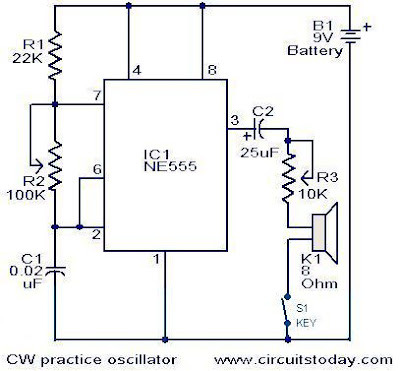
A circuit diagram that can be used for the generation of CW Morse code is shown here.This circuit can be very useful those who would like practice Ham Radio.The circuit is nothing but an astable multivibrator based on NE 555.The frequency of oscillations of the circuit depends on the components R1,R2 & C1.The circuit can be powered from a 9V PP3 battery.
Notes:
- The POT R2 can be used for frequency adjustments.
- POT R3 can be used for volume adjustments.
- The switch S1 can be a Morse code key.
S:circuitstoday.com
Very Low Power 32kHz Oscillator
Circuit diagram:
The base of T1 is biased at 1.25 V using R5/R4 and the reference in IC1. T1 may be any small-signal transistor with a decent beta of 100 or so at 5 µA (defined here by R3, fixing the collector voltage at about 1 V below Vcc). The amplifier’s nominal gain is approximately 2 V/V. The quartz crystal combined with load capacitors C1 and C3 forms a feedback path around T1, whose 180 degrees of phase shift causes the oscillation. The bias voltage of 1.25 V for the comparator inside the MAX931 is defined by the reference via R2. The comparator’s input swing is thus accurately centred around the reference voltage.
Operating at 3 V and 32 kHz, IC1 draws just 7 µA. The comparator output can source and sink 40 mA and 5 mA respectively, which is ample for most low-power loads. However, the moderate rise/fall times of 500 ns and 100 ns respectively can cause standard, high-speed CMOS logic to draw higher than usual switching currents. The optional 74HC14 Schmitt trigger shown at the circuit output can handle the comparator’s rise/fall times with only a small penalty in supply current.
Author: D. Prabakaran - Copyright: 2004 Elekto
Transistor Schmitt Trigger Oscillator
The Schmitt Trigger oscillator below employs 3 transistors, 6 resistors and a capacitor to generate a square waveform. Pulse waveforms can be generated with an additional diode and resistor (R6). Q1 and Q2 are connected with a common emitter resistor (R1) so that the conduction of one transistor causes the other to turn off. Q3 is controlled by Q2 and provides the squarewave output from the collector.

In operation, the timing capacitor charges and discharges through the feedback resistor (Rf) toward the output voltage. When the capacitor voltage rises above the base voltage at Q2, Q1 begins to conduct, causing Q2 and Q3 to turn off, and the output voltage to fall to 0. This in turn produces a lower voltage at the base of Q2 and causes the capacitor to begin discharging toward 0. When the capacitor voltages falls below the base voltage at Q2, Q1 will turn off causing Q2 and Q3 to turn on and the output to rise to near the supply voltage and the capacitor to begin charging and repeating the cycle. The switching levels are established by R2,R4 and R5. When the output is high, the voltage at the base of Q2 is determined by R4 in parallel with R5 and the combination in series with R2. When the output is low, the base voltage is set by R4 in parallel with R2 and the combination in series with R5. This assumes R3 is a small value compared to R2. The switching levels will be about 1/3 and 2/3 of thesupply voltage if the three resistors are equal (R2,R4,R5).
There are many different combinations of resistor values that can be used. R3 should low enough to pull the output signal down as far as needed when the circuit is connected to a load. So if the load draws 1mA and the low voltage needed is 0.5 volts, R3 would be 0.5/.001 = 500 ohms (510 standard). When the output is high, Q3 will supply current to the load and also current through R3. If 10 mA is needed for the load and the supply voltage is 12, the transistor current will be 24 mA for R3 plus 10 mA to the load = 34 mA total. Assuming a minimum transistor gain of 20, the collector current for Q2 and base current for Q3 will be 34/20 = 1.7 mA. If the switching levels are 1/3 and 2/3 of the supply (12 volts) then the high level emitter voltage for Q1 and Q2 will be about 7 volts, so the emitter resistor (R1) will be 7/0.0017 = 3.9K standard. A lower value (1 or 2K) would also work and provide a little more base drive to Q3 than needed. The remaining resistors R2, R4, R5 can be about 10 times the value of R1, or something around 39K.
The combination of the capacitor and the feedback resistor (Rf) determines the frequency. If the switching levels are 1/3 and 2/3 of the supply, the half cycle time interval will be about 0.693*Rf*C which is similar to the 555 timer formula. The unit I assembled uses a 56K and 0.1 uF cap for a positive time interval of about 3.5 mS. An additional 22K resistor and diode were used in parallel with the 56K to reduce the negative time interval to about 1 mS.
In the diagram, T1 represents the time at which the capacitor voltage has fallen to the lower trigger potential (4 volts at the base of Q2) and caused Q1 to switch off and Q2 and Q3 to switch on. T2 represents the next event when the capacitor voltage has risen to 8 volts causing Q2 an Q3 to turn off and Q1 to conduct. T3 represents the same condition as T1 where the cycle begins to repeat. Now, if you look close on a scope, you will notice the duty cycle is not exactly 50% This is due to the small base current of Q1 which is supplied by the capacitor. As the capacitor charges, the E/B of Q1 is reverse biased and the base does not draw any current from the capacitor so the charge time is slightly longer than the discharge. This problem can be compensated for with an additional diode and resistor as shown (R6) with the diode turned around the other way.
Source
Transistor Schmitt Trigger Oscillator The Schmitt Trigger oscillator below employs 3 transistors, 6 resistors and a capacitor to generate a square wa
Transistor Schmitt Trigger Oscillator
The Schmitt Trigger oscillator below employs 3 transistors, 6 resistors and a capacitor to generate a square waveform. Pulse waveforms can be generated with an additional diode and resistor (R6). Q1 and Q2 are connected with a common emitter resistor (R1) so that the conduction of one transistor causes the other to turn off. Q3 is controlled by Q2 and provides the squarewave output from the collector.

In operation, the timing capacitor charges and discharges through the feedback resistor (Rf) toward the output voltage. When the capacitor voltage rises above the base voltage at Q2, Q1 begins to conduct, causing Q2 and Q3 to turn off, and the output voltage to fall to 0. This in turn produces a lower voltage at the base of Q2 and causes thecapacitor to begin discharging toward 0. When the capacitor voltages falls below the base voltage at Q2, Q1 will turn off causing Q2 and Q3 to turn on and the output to rise to near the supply voltage and thecapacitor to begin charging and repeating the cycle. The switching levels are established by R2,R4 and R5. When the output is high, the voltage at the base of Q2 is determined by R4 in parallel with R5 and the combination in series with R2. When the output is low, the base voltage is set by R4 in parallel with R2 and the combination in series with R5. This assumes R3 is a small value compared to R2. The switching levels will be about 1/3 and 2/3 of the supply voltage if the three resistors are equal (R2,R4,R5).
There are many different combinations of resistor values that can be used. R3 should low enough to pull the output signal down as far as needed when the circuit is connected to a load. So if the load draws 1mA and the low voltage needed is 0.5 volts, R3 would be 0.5/.001 = 500 ohms (510 standard). When the output is high, Q3 will supply current to the load and also current through R3. If 10 mA is needed for the load and the supply voltage is 12, the transistor current will be 24 mA for R3 plus 10 mA to the load = 34 mA total. Assuming a minimum transistor gain of 20, the collector current for Q2 and base current for Q3 will be 34/20 = 1.7 mA. If the switching levels are 1/3 and 2/3 of the supply (12 volts) then the high level emitter voltage for Q1 and Q2 will be about 7 volts, so the emitterresistor (R1) will be 7/0.0017 = 3.9K standard. A lower value (1 or 2K) would also work and provide a little more base drive to Q3 than needed. The remaining resistors R2, R4, R5 can be about 10 times the value of R1, or something around 39K.
The combination of the capacitor and the feedback resistor (Rf) determines the frequency. If the switching levels are 1/3 and 2/3 of the supply, the half cycle time interval will be about 0.693*Rf*C which is similar to the 555 timer formula. The unit I assembled uses a 56K and 0.1 uF cap for a positive time interval of about 3.5 mS. An additional 22Kresistor and diode were used in parallel with the 56K to reduce the negative time interval to about 1 mS.
In the diagram, T1 represents the time at which the capacitor voltage has fallen to the lower trigger potential (4 volts at the base of Q2) and caused Q1 to switch off and Q2 and Q3 to switch on. T2 represents the next event when thecapacitor voltage has risen to 8 volts causing Q2 an Q3 to turn off and Q1 to conduct. T3 represents the same condition as T1 where the cycle begins to repeat. Now, if you look close on a scope, you will notice the duty cycle is not exactly 50% This is due to the small base current of Q1 which is supplied by thecapacitor. As the capacitor charges, the E/B of Q1 is reverse biased and the base does not draw any current from the capacitor so the charge time is slightly longer than the discharge. This problem can be compensated for with an additional diode and resistor as shown (R6) with the diode turned around the other way.
Source
Transistor Schmitt Trigger Oscillator
The Schmitt Trigger oscillator below employs 3 transistors, 6 resistors and a capacitor to generate a square waveform. Pulse waveforms can be generated with an additional diode and resistor (R6). Q1 and Q2 are connected with a common emitter resistor (R1) so that the conduction of one transistor causes the other to turn off. Q3 is controlled by Q2 and provides the squarewave output from the collector.

In operation, the timing capacitor charges and discharges through the feedback resistor (Rf) toward the output voltage. When the capacitor voltage rises above the base voltage at Q2, Q1 begins to conduct, causing Q2 and Q3 to turn off, and the output voltage to fall to 0. This in turn produces a lower voltage at the base of Q2 and causes the capacitor to begin discharging toward 0. When the capacitor voltages falls below the base voltage at Q2, Q1 will turn off causing Q2 and Q3 to turn on and the output to rise to near the supply voltage and the capacitor to begin charging and repeating the cycle. The switching levels are established by R2,R4 and R5. When the output is high, the voltage at the base of Q2 is determined by R4 in parallel with R5 and the combination in series with R2. When the output is low, the base voltage is set by R4 in parallel with R2 and the combination in series with R5. This assumes R3 is a small value compared to R2. The switching levels will be about 1/3 and 2/3 of the supply voltage if the three resistors are equal (R2,R4,R5).
There are many different combinations of resistor values that can be used. R3 should low enough to pull the output signal down as far as needed when the circuit is connected to a load. So if the load draws 1mA and the low voltage needed is 0.5 volts, R3 would be 0.5/.001 = 500 ohms (510 standard). When the output is high, Q3 will supply current to the load and also current through R3. If 10 mA is needed for the load and the supply voltage is 12, the transistor current will be 24 mA for R3 plus 10 mA to the load = 34 mA total. Assuming a minimum transistor gain of 20, the collector current for Q2 and base current for Q3 will be 34/20 = 1.7 mA. If the switching levels are 1/3 and 2/3 of the supply (12 volts) then the high level emitter voltage for Q1 and Q2 will be about 7 volts, so the emitter resistor (R1) will be 7/0.0017 = 3.9K standard. A lower value (1 or 2K) would also work and provide a little more base drive to Q3 than needed. The remaining resistors R2, R4, R5 can be about 10 times the value of R1, or something around 39K.
The combination of the capacitor and the feedback resistor (Rf) determines the frequency. If the switching levels are 1/3 and 2/3 of the supply, the half cycle time interval will be about 0.693*Rf*C which is similar to the 555 timer formula. The unit I assembled uses a 56K and 0.1 uF cap for a positive time interval of about 3.5 mS. An additional 22K resistor and diode were used in parallel with the 56K to reduce the negative time interval to about 1 mS.
In the diagram, T1 represents the time at which the capacitor voltage has fallen to the lower trigger potential (4 volts at the base of Q2) and caused Q1 to switch off and Q2 and Q3 to switch on. T2 represents the next event when the capacitor voltage has risen to 8 volts causing Q2 an Q3 to turn off and Q1 to conduct. T3 represents the same condition as T1 where the cycle begins to repeat. Now, if you look close on a scope, you will notice the duty cycle is not exactly 50% This is due to the small base current of Q1 which is supplied by the capacitor. As the capacitor charges, the E/B of Q1 is reverse biased and the base does not draw any current from the capacitor so the charge time is slightly longer than the discharge. This problem can be compensated for with an additional diode and resistor as shown (R6) with the diode turned around the other way.
Source
Negative Resistance Oscillator Circuits

In this circuit, a negative resistance configuration is used to generate the sine wave. The Q1-Q2 pair provides a 15 μA current source. Q2's collector current sets Q3's peak collector current. The 300 kΩ resistor and the Q4-Q5 LM394 matched pair accomplish a voltage-to-current conversion that decreases Q3's base current when its collector voltage rises. This negative resistance characteristic permits oscillation. The frequency of operation is determined by the LC in the Q3-Q5 collector line. The LF353 FET amplifier provides gain and buffering. Power supply dependence is eliminated by the zener diode and the LF353 unity gain follower. This circuit starts quickly and distortion is inside 1.5%.