SCHEMA BATTERY CHARGER Ni-Cd BATTERY AUTO circuit schematic with explanation

SCHEMA BATTERY CHARGER Ni-Cd BATTERY AUTO

SCHEMA BATTERY CHARGER Ni-Cd:
SCHEMA BATTERY CHARGER Ni-Cd BATTERY AUTO circuit schematic with explanation


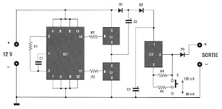
It is a device that can charge any battery Ni-Cd between 4.8 and 1 4.4 Volts with a conventional car battery 1 2 volts. The charging current is constant it can be chosen from the values ​​1 50 20 mA by the selector S.
SCHEMA BATTERY CHARGER Ni-Cd BATTERY AUTO circuit schematic with explanation


This device is very useful for lovers of model making, the video operator, those who use small reception issuance of appliances and all those who use Ni-Cd batteries and need to recharge or network voltage n ' is not available.
SCHEMA BATTERY CHARGER Ni-Cd BATTERY AUTO circuit schematic with explanation


LIST OF ELECTRONIC COMPONENTS: All resistors are of 1/4 watt unless statedotherwise. R = 220Kohms R2 = 1 Kohm R3 = lKohm R4 = 120 ohm 1 watt R5 = 68 ohm 1 watt CI = 10 nF ceramic. C2 = 1000uF16Velec. C3 = 1000yF25Velec. D1 = 1N4001 ... 7 D2-1N4001 ... 7 D3-1N4001 ... 7 T1 = BDX53 T2 = BDX53 IC1 4047 = IC2 = 7805 1 selector 3 Heat Sinks 1 Support 14 pin
Amplificateur audio 6 watts a base de TDA2613 HI FI

6 watt audio amplifier based on TDA2613 HI FI

single scheme electronic audio amplifier 6 watt base TDA2613 HI FI: Description TDA2613: An audio amplifier circuit using 6 watts TDA2613 is shown here. TDA2613 is an integrated Hi-Fi audio amplifier IC Philips Semiconductors system. CI is ON / OFF the click proof, short-circuit, thermal protection and is available online only 9-pin plastic package. In the given circuit TDA2613 is wired to operate from a single supply. Capacitor C4 is the input DC decoupler while capacitors C5, C6 are power filters. Audio input is fed to the inverting input through capacitor C4 not. Inverting input and Vp / 2 pins of the IC are tied together and connected to ground through the capacitor C3. Capacitor C2 couples the speaker to the IC output and the network comprising capacitor C1 and resistor R1 improves the high frequency stability. Amplification Scheme 6 watts using TDA2613:


Notes:. Assemble the circuit on a good quality PCB Supply Voltage (Vs) can be between 15 to 24V DC. A heat sink is necessary to TDA2613. Do not give more than 24V TDA2613. We have over circuits audio amplifiers that may interest you: 1. 30 watts audio amplifier using TDA2040 2. Circuit 10 Watt Audio Amplifier MOSFET 3. car stereo amplifier circuit 4. Watt MOSFET amplifier circuit 50


scheme power amplifier 20W RADIO circuit schemati with explanation

scheme power amplifier 20W RADIO

scheme 20W power amplifier (AUTO BOOSTER FOR CAR-MOTORCYCLE 20 WATTS)

scheme power amplifier 20W RADIO circuit schemati with explanation


The assembly described offers a boost of 20 watts that will allow you to realize a power amplifier with which one can increase the output power of a car radio up to 20 Watts maximum.

scheme power amplifier 20W RADIO circuit schemati with explanation


The input IN is connected to the output of the car radio, output U is connected to the speaker as Represents the scheme.
It is very important to ensure that the speaker has no connection to the chassis ( mass) ; otherwise, integrated circuit IC1, a TDA 2004 would be instantly destroyed.For mounting of components, carefully monitor implementation of the scheme composanls. The alimenlalion will continue at 12 Volts.


LIST OF ELECTRONIC COMPONENTS: All resistors are of 1/4 watt unless statedotherwise. R = 100 Ohms R2 = l, 5Kohms R3 = 180 Ohm R4 = 470 Ohms R5 = 10hmR6 = 10hm Cl = 0, lpFpol. C2 = 1000pFceramique . C3-10uF16Velec. C4 = 0, luFpol.C5 = 0,22uFpol. C6 = 0,22yFpol. C7-0,22uFpol. IC1 = TDA2004 1 Heatsink


FLASHING A SCHEME DOUUBLE BULB CAR AND LOCKS circuit schematic with explanation

Tags

FLASHING A SCHEME DOUUBLE BULB CAR AND LOCKS

FLASHING A SCHEME DOUUBLE BULB CAR AND LOCKS:
FLASHING A SCHEME DOUUBLE BULB CAR AND LOCKS circuit schematic with explanation


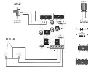
The device allows to flash both lamps simultaneously or alternately.
FLASHING A SCHEME DOUUBLE BULB CAR AND LOCKS circuit schematic with explanation


The Permel DV switch to select the appropriate function, the trimmer TR1 is used to vary the flashing frequency between about 44 and 250 flashes per minute.
The system can be powered by voltages of 12 or 24 Volts DC and the maximum power of each lamp should not exceed 24 Watts if supplies 12 Volts and 48 Watts if supplies 24 Volts.
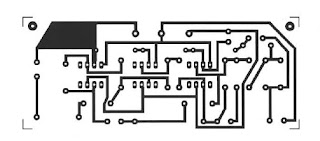
Naturally, if it is powered by 12 volts, the lamps must also be 12 volts; if supplies 24 Volts, the bulbs must be 24 Volts. For the assembly of components and connections, follow the implantation scheme carefully and remember to do both INDICATED bridges on the scheme. The device can be enclosed in a plastic case.


FLASHING A SCHEME DOUUBLE BULB CAR AND LOCKS circuit schematic with explanation


LIST OF ELECTRONIC COMPONENTS All resistors are of 1/4 watt unless statedotherwise. R = 33 ohm R2 = lKohm R3 = lKohm TR1 = 470 Kohm Cl = 100uF25Velec.C2 = 10uF16VeIec. C3 = 4,7uFl6Velec. D1-1N4001 .. .7 T1 = BDX53 T2 = BDX53 IC1 7809 = IC2 = 4017B IC3-40106B 1 Selector 1 contacts Terminal 5 1 Support pin 14 1 Support 16 pin

THEFT SCHEME SIMULATOR FOR AUTOMATIC LED AUTO circuit schematic with explnation

Tags

THEFT SCHEME SIMULATOR FOR AUTOMATIC LED AUTO

SCHEME FOR THEFT AUTO LED A:

THEFT SCHEME SIMULATOR FOR AUTOMATIC LED AUTO circuit schematic with explnation


This is a flashing LED that that is installed on the car dashboard, simulates the presence of a possible alarm system, thereby discouraging the eventual thieves.


Its implementation fonclion is fully automatic: with the motor lights up the LED is extinguished, the engine puts out the LED blinks. The power supply is directly taken from ['electrical installation of the car 12 volt and consumption maximum (flashing LED) is 20 mA only.


THEFT SCHEME SIMULATOR FOR AUTOMATIC LED AUTO circuit schematic with explnation

FOR INSTALLATION MUST PROCEED DELAMANIERE NEXT:. 1) - Connect the point C to the chassis of the vehicle (negative battery) 2) - Connect point A to positifde the battery. 3) - Connect point B to the positive installation as key (eg the positiveof. coil) For those wishing to vary the LED flashing frequency, we must act on the R4 resistance: by increasing its value the frequency decreases and vice versa. For assembly of components and connections, we must be attentive to the implementation of schemes indications.


LIST OF ELECTRONIC COMPONENTS: All resistors are of 1/4 watt unless statedotherwise. R = 2,2Kohms R2 = 220 ohms R3 = lKohm R4 = 33 ohms R5 = 560 Ohms CI = 100 nFceramique. C2 = 100 nFceramique. C3 = 4,7uF16Velec. C4-4,7uF16Velec.Dl = 1N4007 D2 = 1N4007 DZL = 10 volt zener DL1 Red LED = T1 = BC304 IC1 NE555 = 1 Support 8-pin

SCHEMA DOOR ALARM: ELECTRONIC REALIZATION Circuit schematic with explanation

Tags

SCHEMA DOOR ALARM: ELECTRONIC REALIZATION

AUTOMATED ASSEMBLY DOOR RING:
SCHEMA DOOR ALARM: ELECTRONIC REALIZATION Circuit schematic with explanation


When the door is open, the device is triggered during a brief period and activates the buzzer is conneetee him.
SCHEMA DOOR ALARM: ELECTRONIC REALIZATION Circuit schematic with explanation


When the door is closed, the device enters again function by pressing the ring for a few moments. The supply voltage must be 12 Volt DC The maximum consumption is about 70 mA with relay energizes and 3 mA onlyby rest.
To change the relay excitation time (duration of the ring), we must act on the value of the capacity C2. By increasing this value, the time increases and vice versa.
For assembly of components and connections, we must be attentive to the implementation of the scheme indications.


LIST OF ELECTRONIC COMPONENTS: All resistors are 1/4 watt unless otherwise noted. R = 4,7Kohms R2 = 33Kohms Cl = 10uF16Velec. C2 = 470uF16Velec. IC1 = 40106B RL = 2V relay 1 magnetic reed switch 1 Support 14 pin


SCHEMA DOOR ALARM: ELECTRONIC REALIZATION Circuit schematic with explanation

ELECTRONIC BELL: schema and realization Circuit schematic with explanation

Tags

ELECTRONIC BELL: schema and realization

BELL ELECTRONIC SCHEME:

ELECTRONIC BELL: schema and realization Circuit schematic with explanation


The efalimentation voltage is double, it is between -5 and + + -12V (the
dual mount is perfectly stabilized alimentasion)
Pressing and immediately releasing the button, we get a sound whose frequency is determined by the PI adjustment potentiometer. By regulating the potentiometer P2 for his sharp, the circuit
can come into oscillation emitting a continuous whistle. In this case, we must reduce the sound degradation with potentiometer PI. For mounting of components, follow the layout diagram carefully.

ELECTRONIC BELL: schema and realization Circuit schematic with explanation


USTE COMPONENTS All resistors are 1/4 watt unless stated otherwise. R = 68 ohmR2 = lKohm R3 = 10 ohms R4 = 470 ohms R5 = 82 ohms R6 = 22 ohms R7 = 270 ohmsR8 = 10 ohms R9 = 47 Kohm Pl = 4,7MohmsA. P2 = 220 Kohm A. Cl = 22uF16Velec.C2 = luF16Velec. C3 = 0.1 uF 100 Vpol. C4 = 0.047 uF 100 Vpol. C5 = 0.047 uF 100 Vpol. C6 = 0.47 uF 100 Vpol. IC1-741 IC2 = 741 IC3 = 741 P = Push. 3 Supports 8-pin.

ELECTRONIC BELL: schema and realization Circuit schematic with explanation

SCHEMA INTERPHONE 2W circuit schematic with explanation

Tags

SCHEMA INTERPHONE 2W

SCHEMA INTERPHONE 2W:
SCHEMA INTERPHONE 2W circuit schematic with explanation


This is a very useful editing to communicate between two points.


Its operation requires two speakers who will 1'ecoute el has a remission of different messages. Their impedance should be 4 or 8 Ohms.
When the knob is at rest, the speaker A is one that remains in listening; it is therefore installed near the device.
By pressing the button, the speaker Made microphone function while B goes into listening.
The PI potentiometer is used to adjust the volume and therefore the sensitivity. It must be a stabilized voltage of 9 volts to power the assembly. Given its low consumption (about 6 mA at rest), the system can be powered with a standard 9 volt battery. Maximum output power is about 2 Watts. For assembly of components, it must be attentive to the implementation of components scheme.


LIST OF ELECTRONIC COMPONENTS: 
All resistors are 1/4 watt unless otherwise noted. 
R = 560hms 
R2 = 33 ohms 
R3 = 1 Ohm 
Pl 47KohmsB = 
Cl = 220uF16Velec. 
C2 = 100uF16Velec. 
C3 = 100uF16Velec. 
C4 = 100uF16Velec. 
C5 = 270pFceramique. 
C7 = 0, lliFceramique. 
IC1 = TBA820M 
DP = Pushbutton selector. 
TR Transformer. 
1 Support 8-pin.

SCHEMA INTERPHONE 2W circuit schematic with explanation

Circuit prints mounting 2W INTERPHONE

SCHEMA AMPLIFIER 20 WATTS BF 2 WAY Circuit schematic with explanation

SCHEMA AMPLIFIER 20 WATTS BF 2 WAY

SCHEMA AMPLIFIER 20 WATTS BF 2 WAY:


This is an amplifier that feeds a voltage of 14.4 volts, delivers a total power of 20 watts in two different channels which are connected respectively and TWEETER WOOFER.


This amplifier is therefore an active team CROSS-OVER filter with a crossover frequency of 2 kHz.
Each speaker must support a power of 10 watts and have an impedance of 4 Ohms.
The TR1 trimmer allows better rendering dosing acoustide the power of that.Release of acute channel. The supply voltage is governed way of suggestions can be between ages 12 and up get-tive 15 Volts. This amplifier peal also be advantageously used as BOOSTER 2-way car radio. In this case, it is necessary to interpose a resistance of 3.3 ohms between the output of the car radio and I'entree of the amplifier (see diagram). In order to avoid distortions of unpleasant, it is necessary to avoid "applying as input signals of top-50 mV. For mounting of components, you must follow the diagram of allenlivement implanlation.


LIST OF ELECTRONIC COMPONENTS: All resistors are 1/4 watt unless otherwise noted. R = 680 Ohms R2 = 10Kohms R3 = 1 Kohm R4 = 1 Kohm R5 = 10Ohms R6 = 10 ohms R7 = 10hm R8 = 1 Ohm TR1 = 10 Kohm trimmer CI = 5.6 nF ceramic. C2 = 5.6 nF ceramic. C3 = 2,2uF16Velec. C4 = 2,2uF16Velec. C5 = 2,2uF16Velec. C6 = 100uF16Velec. C7 = 100uF16Velec. C8 = 100uF16Velec. C9 = 100nFpol. C10 = 100nFpol. Cll-lOOnFpol. Cl 2 = 2200uF16Velec. IC1 = TDA2004-2005 1 Heat sink.


PRINTED CIRCUIT AMPLIFIER 20 WATTS BF 2 WAY

SCHEMA PREAMPLIFIER WITH LOW INPUT IMPEDANCE Circuit schematic with explanation

SCHEMA PREAMPLIFIER WITH LOW INPUT IMPEDANCE

 SCHEMA PREAMPLIFIER:

SCHEMA PREAMPLIFIER WITH LOW INPUT IMPEDANCE Circuit schematic with explanation


This preamplifier present the characteristic of having a low input impedance, it is therefore perfectly appropriate to be used with magnetic transducers: a low impedance dynamic micro magnetic heads, phone sensors.

SCHEMA PREAMPLIFIER WITH LOW INPUT IMPEDANCE Circuit schematic with explanation


Its amplification is very high, therefore, whether it should be reduced, there should be a series trimmer R3 100 ohms. The system can be powered by a voltage between 9etl8Volts. For its realization, we must
follow the implementation scheme.


LIST OF ELECTRONIC COMPONENTS: All resistors are 1/4 watt unless otherwise noted. R = 1 Kohm R2 = lKohm R3 = 10Kohms R4 = 10Kohras R5 = 10Kohms R6 = 10Kohms R7 = 100Kohms R8 = 100Kohms Cl = 100uF16Velec. C2 = 10uF16Velec . C3 = 4,7uF16Velec. C4 = 47uF16Velec. C5 = 47uF16Velec. T1 BC237 = T2 = BC237 1 clip for 9 volt battery. PRINTED CIRCUIT INPUT PREAMPLIFIER WITH LOW IMPEDANCE


SCHEMA PREAMPLIFIER WITH LOW INPUT IMPEDANCE Circuit schematic with explanation


Simple battery charger with indicator Circuit schematic with explanation

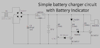
This is a simple 12V rechargeable circuit smart battery charger circuit. You can use it to the best car battery charger circuit battery chargers, inverter battery charger, charger, etc. automatic emergency battery indicator alarm circuit also comes with the battery charger schematic. The main advantage of this indicator is a buzzer informs us when the battery needs recharging. This circuit diagram certainly contributes to your daily life battery charging applications. 
Battery charger diagram:
battery charger with indicator Circuit schematic with explanation

Electronic components: 
-Transformer (230V or 110V to 15V 15V 
T0)-bridge rectifier (1N4007 x 4) 
-condensateur (470uF, 50V) 
- Voltage regulator IC 7815 
-12V rechargeable battery how the circuit this battery charger - The load circuit is constructed. around IC 7815 voltage regulator and two transistors BC 548 - 230V or 110V The main is the first step down using a step down transformer and then it is filtered and rectifiered. - The DC voltage is supplied voltage regulation IC 7815 ;.the output will be regulated 15V 12V rechargeable battery is connected to the output of the voltage regulator. and charge when the main power is available. - When the battery voltage falls below a particular value LED1 stops glowing and buzzer gives her indicating that the battery is discharged and must be charged.

MICRO SPY FM: schema and electronic realization

Tags

MICRO SPY FM: schema and electronic realization


SCHEMA MICRO SPY FM:


The present system allows for an FM transmitter, amplified microphone capsule understood, of small dimensions (23 x 41 mm), which operated in a frequency range between 70 and 1 10 MHz. II can be captured by a single remote FM receiver a few tens of meters.


At the end of improving the scope, it is advisable to apply at A piece of wire 75 cm long that has
an antenna role. A single 9V battery is sufficient to power the system.Consumption is only 5 mA. For mounting of components just carefully follow the instructions in the layout diagram.


LIST OF ELECTRONIC COMPONENTS All resistors are of 1/4 watt unless statedotherwise. R = 10 ohm R2 = 10 ohms R3 = 68 ohms R4 = 120 Ohms CI "100 nF ceramic. C2 = 47 nF ceramic. C3 = 470 pF ceramic . C4 = 3.3 pF ceramic. CV1 = 4- 20 pF variable. LI = 0.6 uH coil. Tl = 2N2222 M = micro Capsule. 1 clip for 9 volt battery.


Technical features:
POWER:. 9VoItsc.c
C0NS0MMATI0N: 5mA
FREQUENCY: 70-110 MHz

scheme timer circuit schematic with explanation

scheme timer circuit schematic


timer scheme:

scheme timer circuit schematic with explanation

This arrangement is of course nothing but a shot but is particularly well suited to
environment "aggressive" of an automobile. As shown in Figure! We use a CMOS door
Schmitt trigger. Pressing the push load instantly Pi Ci condensates which can no longer unload then slowly than in Ffe.Meanwhile the output of the gate Id is at logic low level which saturates Ti and T2 thus feeding the bulbs pilot lights of the vehicle. You will notice indeed that T2 is in fact connected in parallel with the normal ignition from these demieres. The power supply circuit of a car being the seat of violent CAUSED surges, both by the ignition circuit by motors and electromagnets contained in various accessories, zener diodes are DZ2 DZi and to protect the IC from any destruction. The particular position DZ2 is surprising. In fact, it allows to avoid that presented surges on the supply line can reach the exit of IC1 via R5 and the base junction of T1 -emetteur
scheme timer circuit schematic with explanation

Electronic composabtes: IC: 4093 CMOS Ti: A 2N2905 or 2N2907 A T2: 2N3055 DZi, DZ2: zener 15V / 0.4W Ri: 1 Y £ l 1/4 W 5% Cmarron, black, red] RZ 470 kQ 1/4 W 5% [yellow, purple, yellow) R3, R4: 100m / 4W5% Cmarron, black, brown] Rs 6.8 kQ 1/4 W 5% [blue, gray, red] Rg: 4 k l £ 7 1/4 W 5% (yellow, purple, red] The 100 uF / 25V Neck radial chemical information, see text] Cz 100 uF / 25V radial chemicalPi push has work contacts [contact by pressing ] 1 IC 14 has support legs contacts tulips


PIC Programmer Circuit schematic with explanation

Tags
pic programmer: 
What is a PIC ?. Well, like other microcontrollers, it is a small computer with processor, ROM, RAM, and all the I / O circuitry on a single chip. I will focus my projects on PIC that are inexpensive on the market. The chips that I will use will be 16C84, 16F83 and 16F84. These chips are around $ 6.00. Because the ROM inside the chips are electrically erasable, even ICPs can be reprogrammed several times for different types of project. All information stored in the PIC will be held for more than 40 years, without food, until it is electrically erased. Unlike other microcontrollers, the PIC does not require quartz crystals or resonators for their clock, you can simply use a resistor and a capacitor as oscillating elements.
PIC Programmer Circuit schematic with explanation


The project presented here will give you the ability to program a PIC from your parallel printer port on your PC. To program a PIC is relatively simple. A standard supply voltage of 5 volts DC is connected to pin 14 and ground is connected to pin 5. Now bring the voltage on pin 4 to between 12 and 14 volts DC. The data is clocked in one bit at a time by pins 13 and 12. The data itself is sent to the spindle 13. Once the bit is ready, the voltage on pin 12 is raised to 5 volts for the least 0.1 microseconds before being lowered back to earth. The data that were sent to the chip may return out of the chip on the pin 13 to ensure that it accurately. The best way to learn to use this circuit is to actually write a program for the pic and burn it in chip. The first project will be the project of the month in September. So lets get the programmer builds and lets start making plans for the PIC. 

Circuit Schema for flashing the dark with explanation

Tags

Schema for flashing the dark

Electronic flasher Schema:
The electrical diagram of Figure 1 shows the use of four NAND gates contained in the 74HC132 integrated circuit (which may be replaced by the 74LS132). The first three gates IC1-A, IC1-B and IC1-C are used in stage oscillator whose frequency is determined by the C1 values ​​R1 and R2, the third IC1-D is connected in inverter to blink the LED DL1 and DL2.


Circuit Schema for flashing the dark with explanation
Figure 1: Diagram of the night flashing bicycle or pedestrian.


These integrated circuits operating with 5 V and 9 V batteries 6F22 being decidedly convenient, the voltage is reduced and stabilized by a 78L05 regulator.
Turning the R2 cursor from one end of the track to another, flashing pass 0.5 to 3 chips per second.
Circuit Schema for flashing the dark with explanation
Figure 2: Pinouts regulator
78L05 seen from below and LED
side view.


The circuit is installed in a small pocket fi nally lated as a way to put a belt around his waist (cycling, walking, etc.).
You will find it flashing safety is very effi cient in the dark.
There is nothing to prevent the build number (the cost is ridiculous) and arrange them in several places (legs, back, bike, scooter ...) in order to increase visibility.
Circuit Schema for flashing the dark with explanation
Figure 3: Circuit Pinouts
integrated 74LS132 or 74HC132 seen
from above.


List of electronic components:
R1 ............... 2.2 kW
R2 ............... 10 kW trimmer
R3 ..... .......... 220 Ω
R4 ............... 220 Ω
C1 ............... 47 uF electrolytic
C2 ............... 47 uF electrolytic
C3 ............... 47 uF electrolytic
DL1 ............ . diode LED
DL2 ............. diode LED
IC1 .............. SN74HC132 integrated
IC2 ............. . MC78L05 integrated
S1 ............... switch
(Unless otherwise specified, all resistors
are 1/4 W 5%)

OM MICRO RECEIVER TUNING DIODE VARICAP circuit schematic with explanation

Tags

OM MICRO RECEIVER TUNING DIODE VARICAP


SCHEMA OM MICRO RECEIVER TUNING DIODE VARICAP:


This is a great receiver for the range of Medium Wave (500 - 1700 KHz) which is obtained by tuning the potentiometer PI, exploiting the characteristic of the diode DV1.


WARNING!
If using a stereo headset 2 x 32 Ohms, a bridge is realized between the points X. If you use a high standard 8 Ohm speaker, resistor R4 (56 Ohms) is inserted between the points X i1 must be very attentive during the construction of the coil LI to be 60 turns of copper wire enamelled wound on the ferrite bar. The turns must be disposers side by side. It is advisable to start the coil construction by setting the first turn with glue quick setting (cyanoacrylate), then continuing and securing the denier turn with the same type of glue. The coil should be fixed, also with glue a fast setting on the circuit printed respecting a minimum distance of 10 mm between the circuit and the integrated coil. The ends of the terminals will be scraped to remove (email, aulrement it will not be possible to lessoudcrau Circuit prints. For good listening with speaker, the HS 235 can be torque to the HS 140 or another BF amplifier A piece wire a few meters, which serves as an antenna, can be applied at point A. This precaution is generally not necessary thanks to its high sensitivity. The supply voltage must be that of a simple battery 9 V the maximum consumption is 18 mA only.


HOW T'lL:
The emitted AM signals in the range of medium waves are received by the coil LI and PI selected by the potentiometer, the latter role is to apply at the ends of the varactor DV1 according to a specified voltage receiving station. Given that DV1 is a varieap diode, its internal capacity varies with reverse voltage applied, so when the tension is to zero, the capacity is maximum and when the voltage is maximum capacity is the minimum. This amplitude voltage (and therefore of capacity), determined by the potentiometer PI allows the receiver to tune in a range of frequencies between 500 and 1700 KHz. It should be noted that the diode DV1 varieap through C6 and C8 capacitors, is almost in parallel to the coil LI. Zener diode DZ1 provides good voltage stability for control of varieap diode and therefore the responsibility of the syntonic tuning LC group (coil and diode varieap) is represented by the 1'entree system that integrates, thanks to its very high impedance, ensures that Q (quality factor) is high enough canned ensuring good selectivity. The signal then passes through at least three stages of high frequency amplification; Finally. Mid owner detector extracts the signal transistor Low Frequency filter is then applied to the base of a transistor to be amplified.The capacitors C4 and C5 are designed to obtain the maximum discharge of network perturbation signal at 50 Hz. The latter represents the transistor in the circuit structure integrated, whose base is connected to the collector direclement BF amplifier transistor, a a role of impedance adapter of way to ensure a discrete current in the d * listening transducer which should have a 64 ohm impedance is SUPERIOR. That is why when using a headphone 8 Ohms, place in the latter series has a 56 Ohms resistance (56 + 8 = 64). Supply voltage integrated circuit (pins 4 and 6) must be stabilized and DO NOT EXCEED 1.6 Volts. This function is performed by silicon diodes Dl and D2 connected in series and inserted in direct conduction.Their threshold voltage being 700 mV, voltage to their ends (pins 4 and 6 of IC1) can not be superior about 1.4 volts.


LIST OF ELECTRONIC COMPONENTS:
All resistors are 1/4 watt unless otherwise noted. R = 100 Ohms R2 = 1 Kohm R3 = 150 Kohms R4 = 560hms PI = 100 Kohm A. CI = 100 nF ceramic. C2 = 100 nF ceramic . C3 = 100 nF ceramic. C4 = 100 nF ceramic. C5 = 100 nF ceramic. C6 = 10 nF ceramic. C7 = 10 nF ceramic. C8 = 47 nF ceramic. C9 = 180 pF ceramic. Dl = 1N4148 D2 = 1N4148 DVl = BB112Varicap. DZ1 = 7.5 volt zener. IC1 = ZN415E PST = stereo jack socket. lFerrite8X50mm. 1 Support 8-pin.


Advertisement